Reviewed by Lexie CornerMay 21 2025
Researchers John Leo Velpugonda, Matthew Yerich, and Naresh Varnakavi, under the direction of Professor Lih Y. Lin at the University of Washington, have developed a photolithography-based method for patterning solution-processed materials using a dry mechanical lift-off technique. In a recent study published in Light: Advanced Manufacturing, they applied this method to achieve high-resolution patterning of quantum dot (QD) color converters for micro-LED displays.
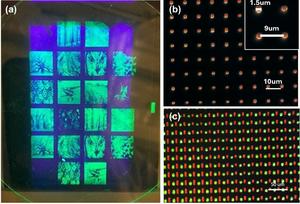
 Micro-patterning of quantum dot color converters using the dry liftoff photolithography method. (a) Fluorescence photograph of a glass wafer displaying different images patterned with green perovskite QDs under a UV lamp. (b) Fluorescence microscope image of patterned red CdSe/ZnS QDs, the inset shows the zoom-in view of patterned features. (c) Fluorescence microscope image of multi-color patterns integrating green perovskite QDs and red CdSe/ZnS QDs. Image Credit: John Leo Velpugonda et al.
Micro-light-emitting diode (micro-LED) display technology holds strong potential for various consumer and industrial applications, including smartwatches, next-generation mobile devices, and augmented or virtual reality headsets.
One of the key challenges in micro-LED development is the miniaturization of individual LED elements. Existing methods, such as labor-intensive pick-and-place techniques or the use of specialized inks, can compromise the optical quality of the pixels.
The newly developed technique is particularly promising because it enables high-resolution patterning of a wide range of solution-processed materials while preserving their optical properties. It also uses the scalability and precision of photolithography.
The process was demonstrated at wafer scale, achieving a patterning resolution as fine as 1 μm. It also proved compatible with red CdSe/ZnS core-shell quantum dots (QDs) and green perovskite QDs, showcasing its broad applicability.
Using this method, the researchers successfully patterned QDs directly onto a blue GaN LED array, achieving integration with a standard LED substrate. As the team notes, this approach offers distinct advantages and could significantly impact the future of micro-LED display manufacturing.
“The method involves using parylene as an intermediary layer, facilitating a dry lift-off procedure in which undesired QDs are mechanically removed without the use of additional solvents. The lift-off QDs can be reused. We achieved a pattern resolution close to 1 µm, which is limited by the capability of the equipment in the fabrication facility.”
“Since the QDs are deposited as the final step and do not undergo any further processing, their photoluminescence properties and narrow linewidth are preserved, making this technique highly attractive for applications requiring precise and reliable patterning of solution-processed materials. Additionally, preserving the optical properties of QDs is crucial for their use in optoelectronic devices, where consistent performance and efficiency are essential,” they added.
The researchers said, “We used this method to create single- and multicolor patterns successfully. The parylene coatings effectively shield the underlying QD films, allowing for the creation of multicolor converter patterns through repeated use of the usual photolithography technique.”
“Furthermore, since the method is agnostic to the materials to be patterned, QDs of different types can be integrated, which was demonstrated by the successful integration of green perovskite QDs with red CdSe/ZnS QDs. The display industry has yet to reach a consensus on the optimum QDs. InP QDs are appealing for being non-toxic, and their optical quality has improved. The universality of the dry lift-off micro-patterning method can ensure agile adaptation to any adopted materials,” they noted.
“Our results demonstrate the versatility of this method for high-resolution micro-patterned solution-processed materials. Its simplicity and effectiveness also make it a promising approach for large-scale manufacturing and integration of QD-based devices, potentially lowering production costs and increasing accessibility for various applications, such as micro-LED displays,” the scientists concluded.
Journal Reference:
Velpugonda, J. L., et al. (2025) A universal high-resolution micro-patterning technique for solution-processed materials. Light: Advanced Manufacturing. doi.org/10.37188/lam.2025.015.