Since the invention of the world's first transistor by scientists at Bell Labs in December 1947, there has been a significant revolution in microelectronics technology that has had a profound impact on lifestyles worldwide. As electronic devices continue to decrease in size, the challenge remains to find an efficient, fast, and cost-effective method for producing micro-nano components.
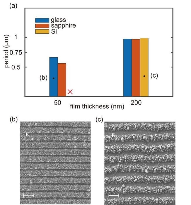
(a) Dependence of LIPSS period on film thicknesses and substrates. SEM images of stationary irradiation-induced periodic nanostructures on different thicknesses of a-Si film: (b) 50 nm on glass and (c) 200 nm on c-Si. Scale bars: 1 µm. Image Credit: Liye Xu, Jiao Geng, Liping Shi, Weicheng Cui, Min Qiu
Conventional methods for direct writing fabrication, including mechanical scribing, focused ion beam etching, electron beam lithography, multiphoton polymerization, and thermal scanning probe etching, suffer from inefficiency. Although techniques like nanoimprinting, photolithography, plasma etching, and scanning laser interference etching can enhance processing speed, they often involve multiple steps such as mask creation or harsh working conditions, and rely on specialized materials.
Utilizing femtosecond lasers to create self-organized periodic surface structures for nano-grating manufacturing has garnered attention. Laser-induced periodic surface structures (LIPSS) employ the interference between incident light and surface electromagnetic waves for material etching, resulting in high processing accuracy.
Furthermore, the self-organized approach simplifies the experimental setup compared to traditional laser interference methods, and the use of a large light spot during scanning significantly boosts fabrication speed.
Researchers, led by Prof. Min Qiu at Westlake University in China, possess extensive research expertise in Laser-Induced Periodic Surface Structures (LIPSS). Their recent findings reveal that inducing a periodic grating on the surface of a thin a-Si film is influenced by the interference of incident light originating from different electromagnetic waves.
When the amorphous silicon film is small (50 nm) and the substrate is a non-silicon material, LIPSS with a small period emerges predominantly under the influence of the slab waveguide mode. In such cases, alterations in substrate material (refractive index changes) lead to corresponding changes in the LIPSS period.
Conversely, when the amorphous silicon film is larger (200 nm), incident light interference occurs with the quasi-cylindrical wave, prompting LIPSS growth through the combined effects of near-field and far-field interactions. In this mode, the LIPSS period is slightly smaller than the laser wavelength and remains unaffected by the substrate material.
The experimental findings are substantiated by numerical simulations based on the Finite-Difference Time-Domain (FDTD) method.
The team's findings were recently published in the journal Frontiers of Optoelectronics.
Journal Reference:
Xu, L., et al. (2023). Impact of film thickness in laser-induced periodic structures on amorphous Si films. Frontiers of Optoelectronics. dx.doi.org/10.1007/s12200-023-00071-6.