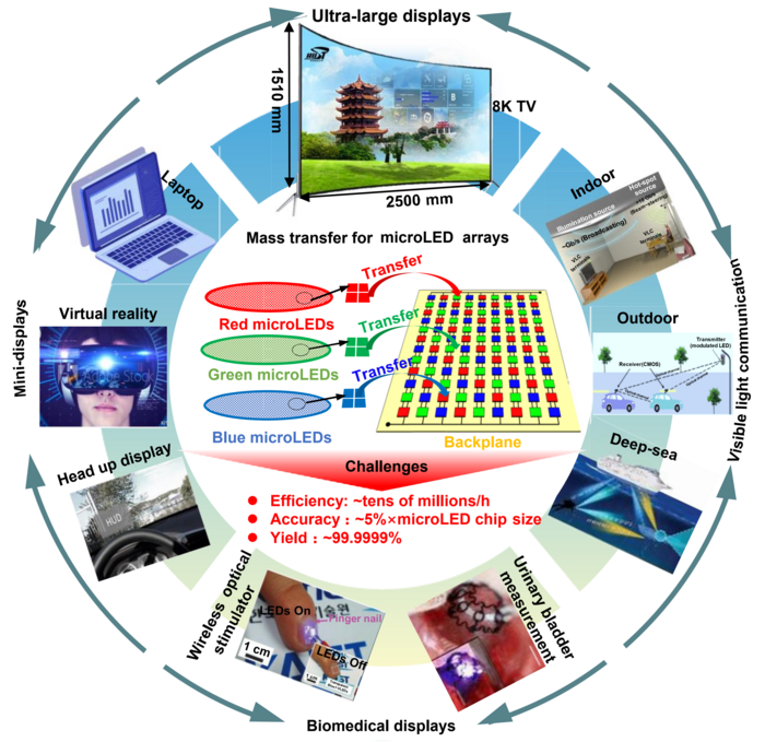
 Figure. l shows the simplified fabrication process of microLED displays (center part in Fig. 1) and representative applications that have been described above. Deterministic assembly of microLED chips from different growth/donor substrates is required. However, since the feature size of microLED chips is <100 µm, there is a trade-off between tiny feature size and fabrication feasibility. There are three enormous challenges. 1) The extreme transfer efficiency (~tens of millions/h) is vital because of their vast numbers. 2) The extreme placement accuracy (~5% of the microLED chip size) is critical for microscale chips. 3) The extreme reliability (~99.9999%) is also essential. In short, traditional assembly methods are not practical for MicroLEDs, and new integration technologies need to be developed. Image Credit: Furong Chen, Jing Bian, Jinlong Hu, Ningning Sun, Biao Yang, Hong Ling, Haiyang Yu, Kaixin Wang, Mengxin Gai, Yuhang Ma and YongAn Huang
Researchers from the State Key Laboratory of Digital Manufacturing Equipment and Technology, Flexible Electronics Research Center, Huazhong University of Science and Technology, PR China, under the direction of Dr. YongAn Huang, have recently published a new study in the International Journal of Extreme Manufacturing that provides a thorough overview of the extreme processes and applications of mass transfer techniques.
The review’s main objective is to discuss the most recent advancements in mass transfer techniques and their numerous uses in microLED displays. The first topic covered was the general assembly procedure for microLED displays and the key issues with mass transfer techniques.
Following that, various advanced mass transfer principles and strategies used in different stages of the production of microLED displays (such as the epitaxial Lift-off technique and pick-and-place technique) are described. Future research opportunities are also discussed in terms of transfer mechanisms, reliability, and cost effects.
An estimate of the upcoming research and applications required for mass transfer is provided by Professor Yongan Huang of the Huazhong University of Science and Technology.
A further in-depth study of interfacial adhesion mechanisms is necessary. The essential relationship between the process parameters and interface reaction (e.g., adhesion strength, fracture mechanics, and chip peeling/flighting state) can undoubtedly provide quantitative guidance for the high reliability of mass transfer.
Yongan Huang, Professor, Huazhong University of Science and Technology
Huang added, “Although lots of small-area transfer schemes have been extensively verified, a further improvement in the reliability, accuracy, and efficiency of large-area transfer techniques is still an area of tremendous opportunities.”
“For achieving high reliability, the development of high precision micro-fabrication/position technologies and material preparations for chips, transfer stamps, and receiver substrates/solders are hotspots. Since lots of mass transfer techniques rely on some specific properties/shapes at specified positions,” he continued.
He further stated, “For example, the fluid self-assembly technique has special requirements for adhesives, which ask for better fluidity, high bonding selectivity between assembled and unassembled surfaces, and acid/high-temperature resistance considering subsequent processes.”
He concluded, “Further exploration of cost-efficient mass transfer techniques is full of challenges as well as opportunities. The development of reversible laser-assisted μTP has important practical significance, which can easily achieve high throughput for large-scale and high-output manufacturing with the help of parallel laser systems and automated platforms.”
Journal Reference:
Chen, F., et al. (2022) Mass transfer techniques for large-scale and high-density microLED arrays. International Journal of Extreme Manufacturing. doi:10.1088/2631-7990/ac92ee.