Nov 29 2017
The problem faced by high-power white light-emitting diodes (LEDs) is the same as that faced by Michigan Stadium on game day, that is, huge numbers of people in a restricted space. Although we do not find people inside an LED, it includes numerous electrons that have to avoid one another and reduce their collisions to keep the efficiency of the LEDs high.
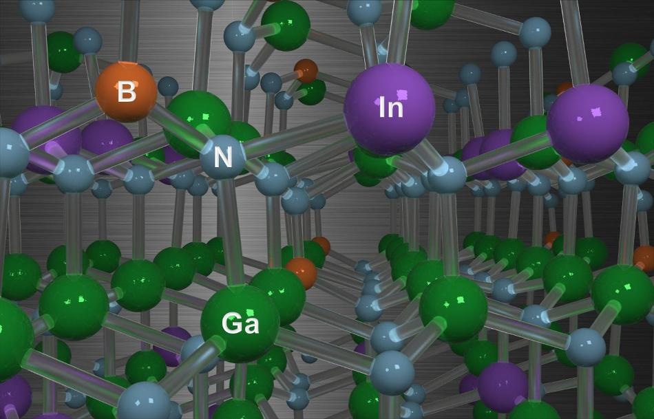 CREDIT: Michael Waters and Logan Williams.
Logan Williams and Emmanouil Kioupakis, researchers from the University of Michigan, adopted high-performance supercomputers and predictive atomistic computations at the NERSC computing facility and have discovered that using boron in the widely used indium-gallium nitride, or InGaN, material can prevent electrons from getting crowded in LEDs, thereby enabling the material to be highly efficient at generating light.
Current LEDs are made of layers of unique semiconductor materials grown one on top of the other. The most basic LED includes three layers. One layer is formed by introducing extra electrons into the material. Another layer is formed with few electrons and includes empty spaces called holes. Lastly, a thin middle layer is sandwiched between the other two layers. The middle layer governs the wavelength of light emitted by the LED. Upon applying an electrical current, the holes and electrons move toward the middle layer in which they combine and generate light. However, if huge numbers of electrons are forced into the middle layer to increase the light emitted by the LED, the electrons tend to collide with one another instead of getting interacting with holes to generate light. Such collisions transform the energy of the electrons into heat through a process known as Auger recombination and decrease the LED efficiency.
One way to overcome this difficulty is to create more space in the middle layer for the holes and electrons holes to move freely. Making the middle layer thicker will scatter the electrons across a broader area, rendering it simple for them to prevent collisions with one another and decreasing the energy lost during the collisions. However, it is not easy to make this middle layer thicker.
Due to the fact that LED semiconductor materials are in crystalline form, the atoms forming the crystals have to be arranged away from each other at uniform distances. This regular arrangement of atoms in the crystals is known as the lattice parameter. While growing layers of crystalline materials on top of each other, the lattice parameters of the layers ought to be similar for exact matching of the regular arrangements of atoms at which the materials are joined, or else the material is deformed to match the underneath layer. Although small deformations are not a major issue, if the top layer is very thick and the deformation gets very big, the atoms get misaligned to such an extent that the efficiency of the LED minimized. At present, the most favored materials for making white and blue LEDs are InGaN enclosed by GaN layers. Regrettably, the lattice parameters of InGaN and GaN do not match, which makes the formation of thicker InGaN layers, for minimizing electron collisions, difficult.
Williams and Kioupakis discovered that when boron is incorporated in the middle InGaN layer, its lattice parameter is altered such that it almost matches that of GaN, and even becomes exactly equal for specific boron concentrations. Furthermore, despite the fact that a completely new element is incorporated in the material, the wavelength of light generated by the BInGaN material is almost equal to that generated by InGaN and can be adjusted to various colors across the entire visible spectrum. This renders BInGaN appropriate to be grown as thicker layers, minimizing electron collisions and enhancing the efficiency of the visible LED.
Apart from the fact the material shows potential for making more efficient LEDs, it should be noted that it can be used in the lab. Williams and Kioupakis have also demonstrated that it is feasible to grow BInGaN on GaN by using the current growth methods used for InGaN, enabling rapid investigation and adoption of this material for making LEDs. Yet, the main difficulty in the application of this study will be to calibrate the best way to include boron into InGaN at adequately greater amounts. However, this study offers a stimulating channel for researchers to investigate the production of innovative LED that are efficient, powerful, as well as being affordable.