Electron microscopy uses a beam of electrons instead of light to illuminate subjects for magnification. The technique has been in use for almost 100 years and is likely to be used at the forefront of scientific research for many more to come.
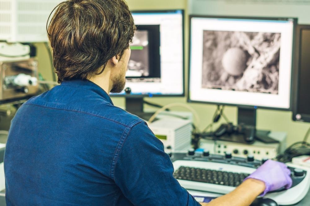
Image Credit: Elizaveta Galitckaia/Shutterstock.com
What is Electron Microscopy?
The American theoretical physics pioneer Richard Feynman called for more powerful electron microscopy as part of his famous 1959 lecture, There’s Plenty of Room at the Bottom.
He challenged the Caltech audience of the American Physical Society’s meeting with a provocative rhetorical question: “Is there no way to make the electron microscope more powerful?”
Feynman was commenting on electron microscopy’s potential to unlock new areas of research for theoretical physics, by enabling us to observe smaller and smaller particles and their reactions with one another.
Unlike conventional optical microscopy, which uses light sources such as lasers to illuminate the subject, electron microscopy employs electron beams.
Magnification is achieved by shaping magnetic fields to create an electron-optical ‘lens’. The curved magnetic field works in an analogous way to the curved glass lenses used in optical microscopy. It ‘focuses’ the beam of electrons to create magnification.
Today, electron micrographs are produced using specialist digital cameras and frame grabbers which capture the images magnified in the electron microscopy system.
The wavelength of an electron is up to 100,000 shorter than that of a photon. Because of this, the theoretical upper limit for electron microscopy magnification is much greater than it is in optical microscopy.
Optical microscopy is limited to around 200 nm resolution due to diffraction. Useful magnification is only possible up to around 2,000 times.
In contrast, the most powerful electron microscopy has achieved resolution better than 50 pm and magnification up to 10,000,000 times.
Electron microscopes are used in research to inspect specimen ultrastructures – the cells and biomaterials that are only visible to electron microscopy. The technique is employed in the study of both biological and inorganic specimens.
In industry, electron microscopy is widely applied in quality control and failure analysis functions.
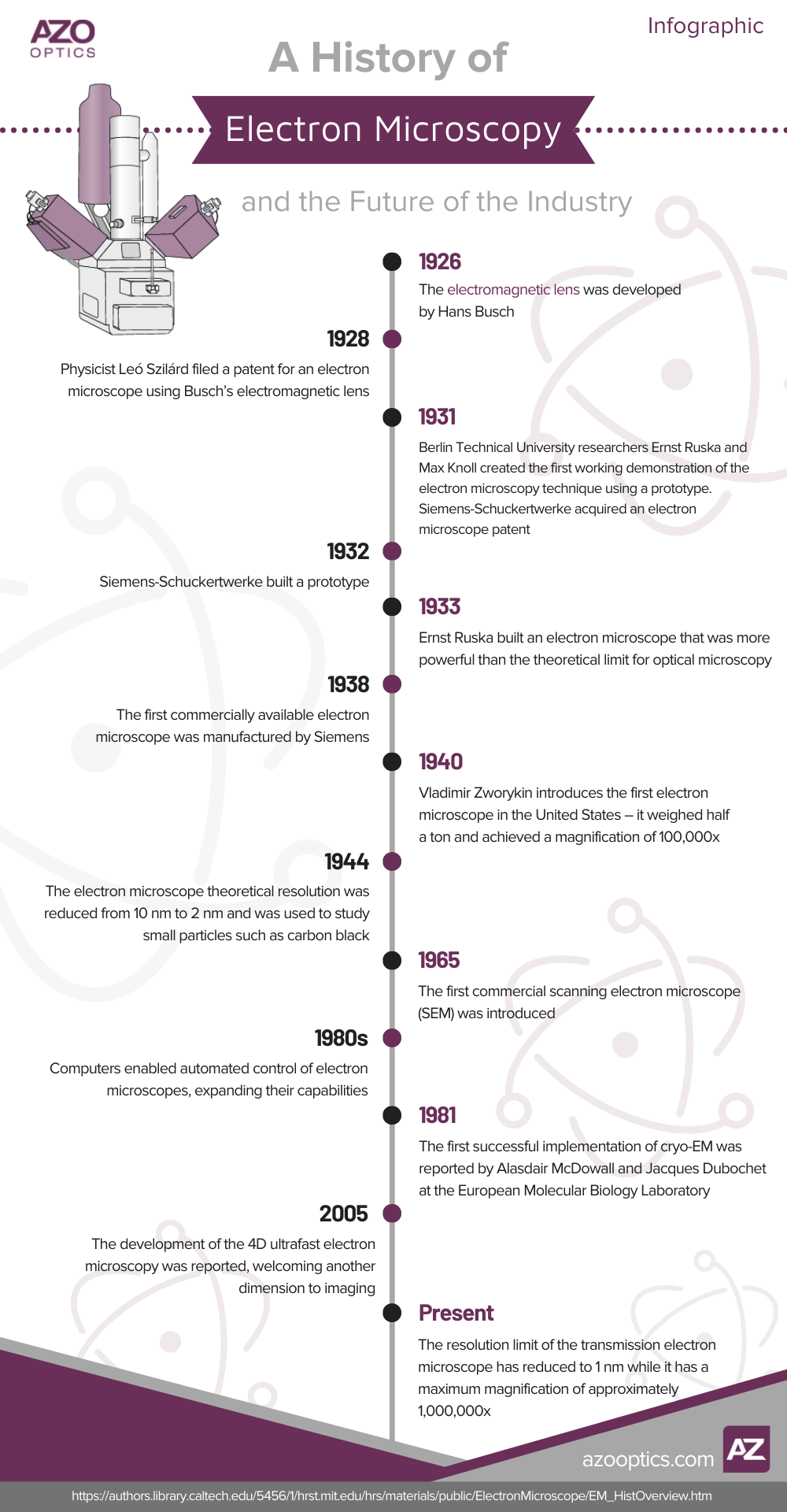
Image Credit: Sara Lopez Segura
The electromagnetic lens – a curved magnetic field that works in an analogous way to glass lenses in optical microscopy – was developed by Hans Busch in 1926. Two years later, physicist Leó Szilárd filed a patent for an electron microscope using Busch’s electromagnetic lens.
Berlin Technical University researchers Ernst Ruska and Max Knoll – a physicist and an electrical engineer, respectively – created the first prototype electron microscope in 1931. This machine, which achieved 400 times magnification, was the first working demonstration of the electron microscopy technique.
Siemens-Schuckertwerke (now global engineering company Siemens) acquired an electron microscope patent in the same year, and in 1932 the company built a prototype.
In 1933, Ruska built an electron microscope that was more powerful than the theoretical limit for optical microscopy. Siemens manufactured the first commercially available electron microscope in 1938.
The Future of Electron Microscopy
Today, electron microscopy is used to study ultrafast processes, magnify specimens to atomic-scale resolution, and measure nanotechnology functionality.
Ferromagnetic and ferroelectric nanostructures are studied using electron microscopy techniques as they can be viewed in situ with these methods. This is attributable to the requirement for a continuous decrease in element size in non-volatile memories.
Electron microscopy is used at the cutting edge of quantum physics research today. The atomic, electronic, and spin structures that form objects at the nanoscale of size can only be studied with powerful electron microscopes. Graphene, weak scattering objects, and single-wall carbon nanotubes can only be effectively studied with electron microscopy.
The latest development in electron microscopy – ultrafast imaging and diffraction – has opened new borders for the study of these structural dynamics at the nanoscale. Using femtosecond short electron pulses, this technique allows for electronic and atomic motion to be detected on their natural timescales.
The future of electron microscopy will see more use in dynamic analysis like this. Applications include the study of energy transfer and heat transfer, which could unlock better ways of storing and transporting energy in the future.
Electron Microscopy (TEM and SEM)
Video Credit: Professor Dave Explains/YouTube.com
References and Further Reading
Kruger, D.H., P. Schneck and H.R. Gelderbloom (2000). Helmut Ruska and the Visualisation of Viruses. Department of Medical History. [Online] https://doi.org/10.1016/S0140-6736(00)02250-9
Rudenberg, H. Gunther and Paul G. Rudenberg (2010). Origin and Background of the Invention of the Electron Microscope. Advances in Imaging and Electron Physics. [Online] https://doi.org/10.1016/S1076-5670(10)60006-7
Zhu, Yimei and Hermann Dürr (2015). The Future of Electron Microscopy. Physics Today. [Online] https://doi.org/10.1063/PT.3.2747
Disclaimer: The views expressed here are those of the author expressed in their private capacity and do not necessarily represent the views of AZoM.com Limited T/A AZoNetwork the owner and operator of this website. This disclaimer forms part of the Terms and conditions of use of this website.