Key Takeaways
- Lithography is essential for accurate, flexible, and efficient microlens array production.
- It supports the creation of complicated designs for advanced applications such as laser beam shaping.
- Grayscale and direct laser writing lithography (DLWL), among other techniques, improve efficiency and customization.
- Avantier uses this technology to fabricate high-quality, tailored microlens arrays.
Lithography is a critical technique in the production of microlenses. It enables the precise manufacturing of many of the world’s highest quality and most advanced microlens arrays.
This overview examines the role of lithography in microlens array fabrication and illustrates how lithographic techniques can be applied by world-class optical manufacturing companies such as Avantier.
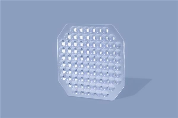
Microlens arrays are important in the modern world, and lithography is one of their most promising fabrication techniques. Image Credit: Avantier Inc.
Why Lithography
All microlens arrays must meet strict and specific production requirements, such as high uniformity over large areas. For certain applications, especially those involving manufacturing on curved or flexible surfaces, the requirements are even more complex.
Lithography is a valuable technique in microlens array production because it offers:
- Accuracy: Lithography facilitates consistent, precise fabrication of well-defined, multi-level structures. For example, it can manufacture 2 x 2 square centimeter arrays with feature sizes as small as 2 µm.
- Flexibility: Various lithography methods can be used to create microlens arrays with diverse symmetries, structures, and sizes. Many lithographic techniques are also easily customized, allowing manufacturers like Avantier to produce arrays that meet specific application requirements.
- Efficiency: Lithography is an inherently efficient process. Specific techniques, such as DLWL, can be used to rapidly pattern large areas for high production speeds.
- Cost effectiveness. Although cost ratios vary depending on the specific lithographic method used, some approaches, including the use of transparency films as grayscale masks, can reduce production time and complexity, lowering manufacturing costs.
- Suitability for Sophisticated Applications: Laser beam shaping and wavefront sensing require intricate microlens array designs, which can easily be produced with contemporary lithography methods.
However, lithography is not a one-route production process; there is a broad array of methods and materials available that allow optical designers to optimize both the production process and the resulting arrays.
An early stage in the MLA design process involves in-depth modeling of anticipated interactions between a specific type of photoresist and propagated light. Different photoresist and substrate materials can be chosen based on desired outcomes.
Below are two methods that can be used to fabricate microlens arrays with non-spherical geometries.
A Closer Look: Grayscale Lithography
Producing non-spherical microlens arrays with lithography is usually a multi-step, iterative process involving binary masks and reactive ion etching to form multi-level structures in photoresist. The n-level structures are created using conventional techniques, n repetitions of photolithography, and careful attention to alignment ensures the arrays act as analogs of continuous 3D structures.
Grayscale lithography is one technique that can, in some cases, significantly boost fabrication efficiency. It replaces binary masks with grayscale photomasks (for example, halftone chrome masks or high-energy beam sensitive glass masks), allowing control over light intensity. This approach enables the formation of 3D structures in just a single exposure.
The masks transfer patterns onto the photoresist without reducing size, so they must be prepared at the appropriate micrometer scale. However, they can be fabricated from large-scale transparency films using microlens arrays to reduce their size.
A Closer Look: Direct Laser Writing Lithography
Direct laser writing lithography (DLWL) is another contemporary lithography method that shows promise for fabricating aspheric microlens arrays. This technique supports versatile design, a customizable filling factoring arbitrary off axis operation for each microlens, and simplifies manufacturing.
DLWL is best-suited for large-scale fabrication at high precision levels. A 2022 study using 12-bit direct laser writing lithography demonstrated high manufacturing speed, excellent lens shape control, and average surface roughness below six nanometers.
Lithography for Microlens Array Fabrication at Avantier
Avantier leads in microlens array fabrication, using cutting-edge equipment and lithography expertise to manufacture high-quality, precision arrays tailored to client needs. Avantier’s expert designers provide detailed modeling of light propagation and photoresist interactions, helping clients select suitable materials based on their desired outcomes.
References and Further Reading:
- Luan, S., et al. (2022). High-speed, large-area and high-precision fabrication of aspheric micro-lens array based on 12-bit direct laser writing lithography. Deleted Journal, 3(4), pp.1–1. https://doi.org/10.37188/lam.2022.047.
- Wu, H., et al. (2002). Reduction Photolithography Using Microlens Arrays: Applications in Gray Scale Photolithography. Analytical Chemistry, 74(14), pp.3267–3273. https://doi.org/10.1021/ac020151f.
- Yao, J., et al. (2003). One-step lithography for fabrication of a hybrid microlens array using a coding gray-level mask. Proceedings of SPIE - The International Society for Optical Engineering, (online) 4945, pp.130–137. https://doi.org/10.1117/12.468419.
- Yuan, W., et al. (2018). Fabrication of Microlens Array and Its Application: A Review. Chinese Journal of Mechanical Engineering, 31(1). https://doi.org/10.1186/s10033-018-0204-y.

This information has been sourced, reviewed, and adapted from materials provided by Avantier Inc.
For more information on this source, please visit Avantier Inc.