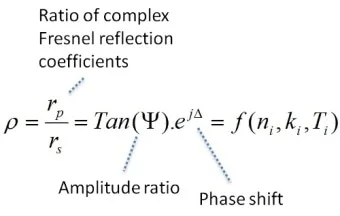
Measured ellipsometric parameters (Ψ and Δ) will provide information on the physical properties of the layer structure under analysis. These measurements provide information on the layer’s thickness and refractive index and are an important part of the fundamental equation of ellipsometry.
The equation is transcendental and highly nonlinear, meaning that numerical methods on a model-based perspective should be used to solve this equation. During this method, layer structure is analyzed in terms of the thickness and the model’s optical functions.
Relative phase shift is measured, and this is compared with measured quantities via a numerical regression process.
Optical Modeling
A loose optical model of the structure must be deciphered as part of the numerical regression process. This usually involves a substrate being estimated using a thick semi-infinite material with known optical characteristics.
Parametric functions tend to be used to outline each layer’s spectral absorption and dispersion. Basic empirical formulas can be utilized for some materials, while others require the use of more multifaceted definitions.
In instances where a parametric function occurs (such in the case of the Cauchy law), dispersion is parametrized by several values, including A, B and C.
These parameters are considered useful when regression has already taken place, and collecting these at the end of the regression process will allow the refractive index to be measured as a function of wavelength.
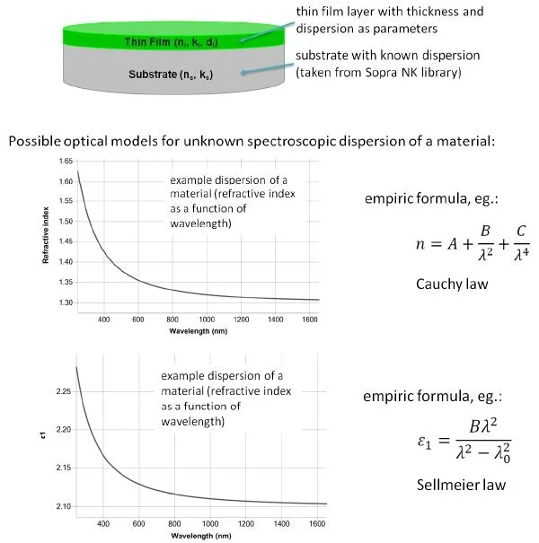
Image Credit: Semilab Semiconductor Physics Laboratory
The Sellmeier model offers an alternative means of modeling the dielectric function. While the Cauchy law is an empirical formula, the Sellmeier model is based on a zero linewidth Lorentzian absorption peak that is found some distance from the range of measurement at peak position λ0 and oscillator strength B.
Because of this, the film shown here would have no optical absorption within the wavelength range being measured.
The Sellmeier model’s hyperbolic-shape can be equal to the shape acquired via the Cauchy model. The Sellmeier model offers the key advantage that it is easy to combine with other dispersion formulas refined for complex dielectric functions; for example, Drude, Gauss, or Lorentz.
This approach is also useful for wider wavelength range modeling while offering users the ability to capture more than one Sellmeier peak in a single model.
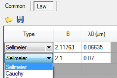
SEA software selection of dispersion law types in Structure tab. Image Credit: Semilab Semiconductor Physics Laboratory
Performance of Dielectric Film Measurement
When measuring optically transparent films, sensitivity can range from sub-nanometers to several tens of micrometers. The simulation result shown here demonstrates sub-nm sensitivity; for example, the SiO2 covered Si substrate present in the Δ curve is above the 600 nm wavelength.
The higher limit for the determination of dielectric film thickness will depend on the maximum resolution and wavelength range of spectroscopic ellipsometer instrument being used.
For example, when glass substrate is utilized, the refractive index variation between the thin film coating and the substrate will be significantly lower in the SiO2 and Si sample structures.
Glass or SiO2 measurements necessitate the use of instruments that are sensitive enough to optically distinguish between two similar dielectrics. Semilab’s rotating compensator ellipsometer is capable of measuring SiO2 thickness on glass sheets, even in cases where the thickness range is as low as <50 nm.
This application method has become increasingly relevant within the flat panel display industry. The oxide coating on these devices acts as an initial buffer layer, meaning that it must be evenly deposited across panels of glass that are several m2 in size.
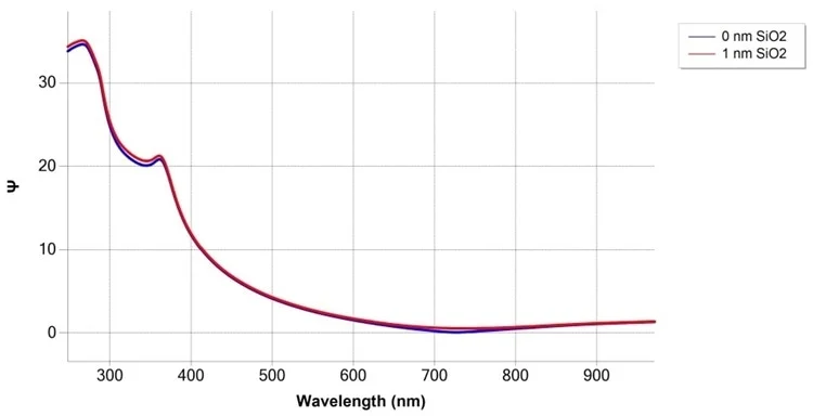
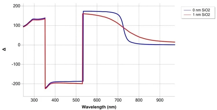
Simulation of SiO2/Si measurement at 75° angle of incidence, with and without 1 nm SiO2 film. Image Credit: Semilab Semiconductor Physics Laboratory
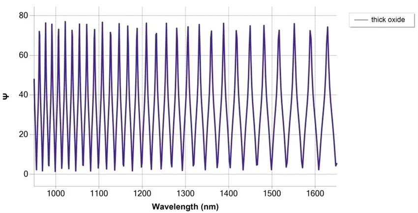
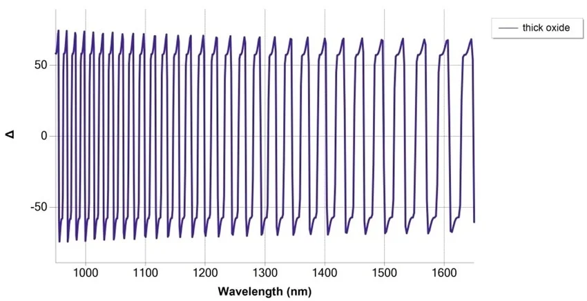
Simulation of SiO2/Si measurement at 75° angle of incidence, with thickness 30 μm with NIR fast detection spectrograph. Image Credit: Semilab Semiconductor Physics Laboratory
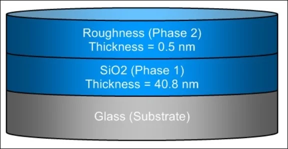
Optical model result output for the sample structure of thin SiO2/glass. Image Credit: Semilab Semiconductor Physics Laboratory
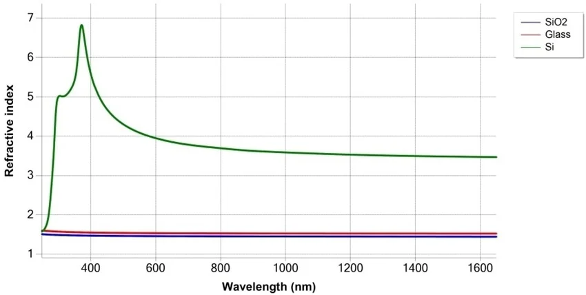
Refractive index difference for SiO2 layer vs. glass or Si substrates. Image Credit: Semilab Semiconductor Physics Laboratory
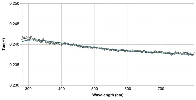
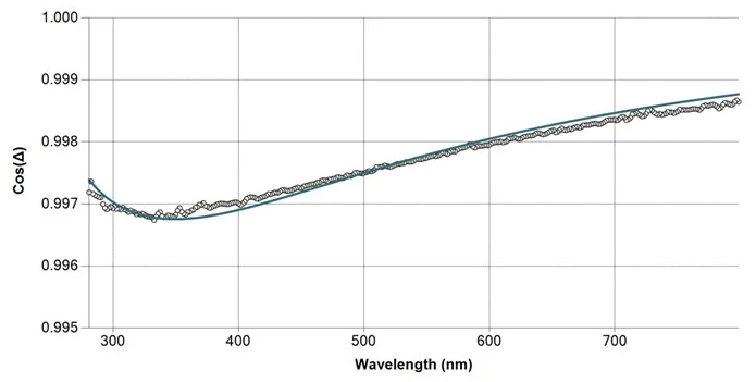
Measured and fitted spectrum of thin SiO2/glass sample at 65° angle of incidence. Image Credit: Semilab Semiconductor Physics Laboratory

This information has been sourced, reviewed and adapted from materials provided by Semilab Semiconductor Physics Laboratory.
For more information on this source, please visit Semilab Semiconductor Physics Laboratory.