Reviewed by Lexie CornerMay 29 2025
A research team from Nanjing University in China has developed a novel method that significantly improves the performance of metalenses for microscopy applications. Their study introduces a metalens-based microscope that achieves high-resolution imaging and a wide field of view within a compact design.
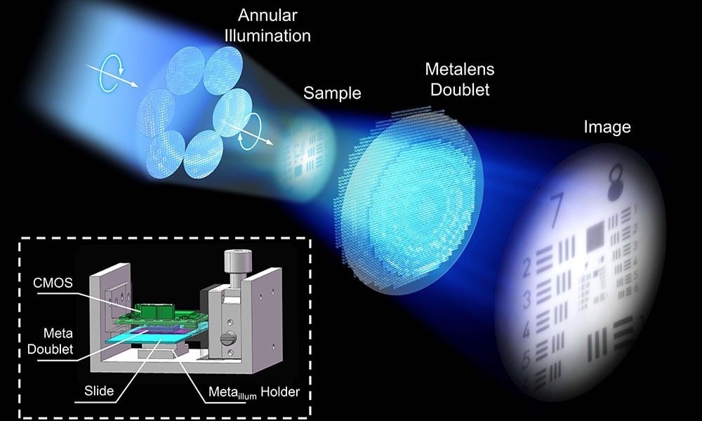
 The proposed metalens doublet configuration with annular illumination can overcome off-axis aberrations and achieve unprecedented high-resolution wide-field imaging, even in a compact and highly integrated prototype. Image Credit: Tao Li and Jiacheng Sun, Nanjing University
Metalenses are a newer type of lens in optical technology. Unlike traditional microscope lenses that use curved glass, metalenses use tiny structures to control light on a very small scale. Because they are thin, flat, and lightweight, metalenses are a good fit for small imaging systems and electronic devices.
However, metalenses still face challenges when used in microscopes. One of the main problems is off-axis aberration, which reduces both image quality and the size of the area that can be clearly seen.
So far, metalenses haven’t matched the performance of regular microscope lenses. Some designs can create sharp images, but only within a very small viewing area, which limits their usefulness.
To solve this, the researchers used two metalenses placed on opposite sides of a clear piece of silica, along with a special type of lighting called annular illumination. The metalenses are made of tiny silicon nitride structures, shaped and spaced very precisely.
This setup helps reduce image distortion and improves resolution, leading to better overall image quality.
Our metalens microscope, featuring a FOV of up to 150 μm and a half-pitch-resolution of 310 nm, far exceeds the highest resolution ever reported in meta-microscopy.
Dr. Tao Li, Study Corresponding Author, Nanjing University
This work marks a significant improvement, as the researchers were able to see details that earlier metalens systems could not detect.
To demonstrate how their method works in practice, the team built a compact prototype. The device has a 1 mm field of view and a resolution of 620 nanometers. The design uses metasurfaces not only for imaging but also for circular lighting, which helps keep the system small. The finished microscope is much smaller and lighter than traditional models, measuring just 4 cm × 4 cm × 5 cm.
The researchers used the meta-microscope to examine cervical cancer cells. It successfully captured images showing different stages of cancer development within the same viewing area, including important cell features like nuclear growth, changes in shape, and division. Being able to see these features across a wide field of view could help medical professionals better understand tissue samples and potentially improve diagnosis.
Our experimental results demonstrate high-quality microscopic bioimages that are comparable to those obtained from traditional microscopes within a compact prototype, highlighting its potential applications in portable and convenient settings.
Dr. Tao Li, Study Corresponding Author, Nanjing University
This technology could be useful in many situations where both portability and high-quality imaging are needed. Possible uses include medical imaging in low-resource settings, mobile monitoring equipment, and outdoor research where regular microscopes are difficult to use.
The method could also be built into small electronic devices, which may make it useful for future technologies, including advanced medical or laboratory automation tools.
Overall, this development is an important step toward making metalens-based imaging systems that work as well as traditional optics, but with added benefits like smaller size, lower weight, and easier integration. It also opens the door to new compact imaging tools and other high-performance optical devices using metasurfaces.
Journal Reference:
Sun, J. et al. (2025) High-resolution and wide-field microscopic imaging with a monolithic meta-doublet under annular illumination. Advanced Photonics. doi.org/10.1117/1.AP.7.4.046006