MicroLEDs continually demonstrate performance benefits for displays, including higher contrast and brightness, greater pixel density and wider color gamut. MicroLEDs facilitate enhanced visual performance in ambient light conditions, from complete darkness to broad daylight and when viewed from multiple viewing angles.
These characteristics make microLEDs particularly attractive for applications including mobile phones and smart-watches, automotive display panels, augmented and mixed reality (AR/MR) headsets and digital signage.
Manufacturing high quality microLED panels is a persistent challenge that often limits production efficiency. Before manufacturers can deliver commercially viable microLED display products, there are certain quality issues to consider.
The Challenge of MicroLED Display Uniformity
As self-emissive elements, microLEDs are independently driven, in which the variability can be severe between luminance and color (see Figures 1 and 2). This variability is easily detected by the human eye, rendering visual performance unacceptable in the resulting displays.
Figure 1. This close-up image of a microLED microdisplay panel demonstrates the potential luminance and color uniformity issues resulting from varying microLED pixel output across the display. Image Credit: Radiant Vision Systems
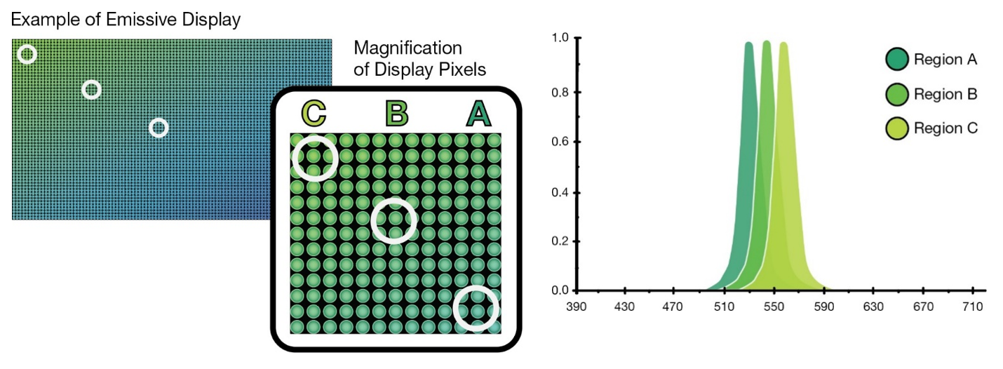
Figure 2. Illustration of an emissive display with color variability (far left), with magnification of display pixels A, B and C at different points on the display (center left); example of varying spectral data for A, B and C (right). Image Credit: Radiant Vision Systems
Variability is further complicated by the fact that each microLED is a monochromatic subpixel (usually red, green, or blue) whose output merges with other subpixels to generate the total brightness and color of a single display pixel.
This variability at the subpixel and pixel level presents an irregular appearance across the display, leading to a low yield of displays deemed acceptable, as well as costly rework and the rejection of expensive components.
Measurement of microLED subpixels is crucial in order to evaluate, quantify and correct display pixel output. Yet, it is challenging to measure microLEDs with great accuracy due to their variability, proximity, size and quantity per display.
This makes correction an equally challenging prospect at the speed necessary to facilitate commercial production throughput demands.
Correcting Emissive Displays
Display manufacturers have persistently used correction methods (electronic compensation or calibration) to enhance visual quality.
A straightforward concept: by adjusting the inputs to individual subpixels of an emissive display, pixels previously identified as dim can be modified to a uniformed luminance level at each bright state, resulting in consistent brightness and color appearance across the display at all states.
Firstly, display correction initially requires having in-display electronics that can manage inputs to the individual subpixels and enable adjustments based on the correction factors that have been calculated for each subpixel.
Secondly, a measurement system is necessary to quantify individual subpixel luminance and chromaticity values accurately and calculate distinctive correction factors for each subpixel at each bright state.
This technique was initially developed for the calibration of LED video screens and has been modified for today’s high resolution emissive displays (OLED and microLED) utilizing a correction technique known as ‘demura’ or pixel uniformity correction (PUC).
Demura
The demura method follows three specific steps:
- To calculate luminance values at each pixel coordinate location, use a high-resolution imaging colorimeter to measure each subpixel in the display. Test images are fed to the display to pinpoint subpixels of each color set. These images allow the computation of measurement and correction factors in each set. For instance, a green test image can be fed to the display to illuminate every green subpixel. An imaging colorimeter measures and records each green subpixel’s output. This process is duplicated for all primaries (red, green, blue) and, typically, white.
- Into a coefficient calculator, load measurement data from each display pixel’s coordinate position. Utilizing test analysis software, correction factors are calculated to normalize luminance and chromaticity discrepancies between pixels in the display.
- Apply correction factors to the signals of each subpixel at each pixel location utilizing an external control IC (integrated circuit) system.
Considerations for MicroLED Measurement
Different display metrology systems have their own particular set of advantages and disadvantages when applied to microLED subpixel measurement.
For example, a spectroradiometric system has great measurement accuracy (both luminance and chromaticity), but slow cycle times render it an inefficient solution to measure the millions of pixels that make up a complete microLED display.
In addition, spectroradiometric systems generally have a spot size that is too big to give the most precise measurements of individual microLED emitters. A standard microLED measures <100 micrometers (µm) square, and <50 µm is relatively common, with some as small as 3 µm1 (see Figure 3).
A measurement system with the capacity to measure structures with a diameter down to 0.075 mm, such as a spectroradiometer, would be inappropriate when differentiating and measuring the characteristics of singular microLEDs usually smaller than 75 µm.
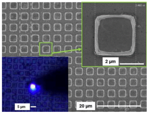
Figure 3. SEM micrograph of 3-µm size / 5-µm pitch microLED array. Inset lower left is an optical photograph of a microLED powered on. Image Credit: Leti
To achieve production takt time requirements, high speed machine vision cameras are occasionally employed for automated visual display inspection. Yet, these systems do not intrinsically offer photometric and colorimetric accuracy necessary to quantify variables in luminance and chromaticity values, largely at the subpixel level.
A calibrated, high resolution imaging colorimeter supplies both the speed and accuracy required to meet production needs and thus provides an efficient solution for pixel- and subpixel-level measurement of microLEDs in production. A measurement solution optimized for microLED test and correction would be comprised of:
- Imaging Colorimeter: The benefits of imaging colorimeter and photometer systems blend efficiency - the capacity to detect all significant variations across displays in a single image, achieving several measurements at once: contrast, chromaticity, luminance, pixel defects, uniformity, etc. Another benefit is scope - the capacity to record a display’s complete field of view (FOV) in a single image, just as the end-user sees the device. An imaging colorimeter measures luminance and chromaticity, while an imaging photometer measures luminance.
- High Resolution: A microLED measurement system demands high resolution imaging capabilities. High resolution imaging facilitates the precision necessary to identify and isolate each pixel and subpixel for measurement and the efficiency for a single image to record values for every pixel across progressively high resolution and pixel-dense displays.
- Low Noise: Image noise (which can include shot noise, read noise, or electronic noise) impedes image clarity image. Regardless of how high the imaging systems resolution (the number of megapixels (MP) of its sensor), if significant noise is captured by the system, per sensor pixel (yielding low signal-to-noise ratio, or SNR), then the system’s resolution may be effectively much lower.
- Calibration: To conduct precise measurements in line with CIE standards, careful calibration of a metrology device is necessary. A well-known method utilizes reference data captured by a spectrometer to calibrate the imaging colorimeter’s response. Enhanced Color Calibration™ (ECC) is an algorithm-based calibration method proven to enhance the accuracy for sources with high variability (see below, the Enhanced Color Calibration section).
- Test & Analysis Tools: Image processing software allows manufacturers to hone and perform tests on a captured image. Preferably, an analysis package for display measurement would be incorporate the tools needed to detect and quantify luminance, pixel & line defects, contrast, chromaticity, uniformity, display mura and other characteristics. Algorithms to enhance imaging accuracy for subpixel registration and measurement are advantageous features that improve display test efficiency when included in out-of-the-box solutions.
The Importance of Measurement Accuracy: Luminance and Chromaticity
In 1931, the Commission Internationale de L’éclairage (CIE) established a standard for the scientific quantification of the physical properties of color a human observer perceives, allowing for precise mathematical representation and reproduction of colors (Figure 4).
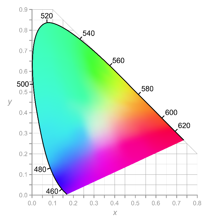
Figure 4. A graphical representation of the CIE 1931 color space, including all colors visible to the human eye. The black numbers on the edge give the visible spectrum in wavelengths, while perceived colors are represented as coordinate points (x and y) within these limits. Image Credit: Radiant Vision Systems
When measuring highly variable microLEDs, it is necessary that a measurement system can discern color variation with equivalent sensitivity to the human eye in order to ensure good accuracy.
A standard human spectral sensitivity is evaluated using the mathematical formula of the CIE standard to supply chromaticity values as coordinates within the CIE color space.2
Tristimulus (XYZ) color filters on a rotating filter wheel allow imaging systems to carry out color measurement in line with CIE color-matching functions and chromaticity values. Light passing into the metrology device is fed through the respective filters and then recorded by a sensor (see Figure 5).
The filters modify the incoming light, blocking particular wavelengths to ensure a measurement image with values that are as close as possible to what the human eye perceives is captured by the sensor.
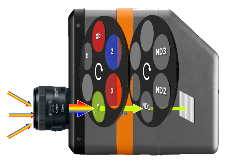
Figure 5. A CIE-matched tristimulus filter wheel system (shown here inside a ProMetric® I-series Imaging Colorimeter from Radiant Vision Systems) enables a measurement device to capture light and color as values that reflect the spectral sensitivity of the human eye. Image Credit: Radiant Vision Systems
Tristimulus Systems: A 2020 study by Jensen, Piehl and Renner3 shows that the tristimulus filter wheel system demonstrated a high degree of accuracy for CIE standard color measurement (for details, see below, the section titled Measurement Accuracy Study: Tristimulus System).
Enhanced Color Calibration™: All imaging systems used for metrology applications call for calibration data from a spectrometer or other device to verify the accuracy of the measurements. Enhanced Color Calibration (ECC) from Radiant Vision Systems supplied the greatest level of color measurement accuracy using state-of-the-art calibration algorithms.
The ECC method generates a 12-element correction calibration matrix to optimize the capacity of the color measurement system in order to withstand variability (supply accurate color measurement across a large area of the CIE color space) from a calibration point (calibrated color value; see Figure 6).
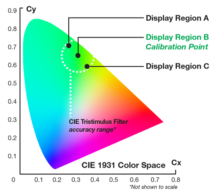
Figure 6. ECC enables a tristimulus imaging colorimeter to continue to provide accuracy even as source spectral data deviates further from the calibration point. This chart illustrates an expected accuracy limit (area within the white dotted line circle) for a tristimulus imaging colorimeter for measuring display pixels A, B and C plotted from Figure 2. Image Credit: Radiant Vision Systems
Measurement Accuracy Study: Tristimulus System
The below study assesses the color measurement accuracy of a tristimulus-filter-based imaging colorimeter system utilizing ECC (Radiant Vision Systems ProMetric® I29 (29MP) Imaging Colorimeter) versus a reference meter (a spectroradiometer). LEDs of various colors were measured by the reference meter and by the imaging colorimeter.
First, calibration of the imaging colorimeter was set to a base output for each LED (using ECC). Then, each LED was measured by each system as its output was varied (LED variability was introduced by providing different current levels).
The accuracy of the imaging colorimeter was determined by its capacity match reference meter measurements as chromatic distance of the LED output increased from the system calibration point.
Results: The measurement data plotted in Figures 7 and 8 reveal that a tristimulus system can supply accurate luminance and chromaticity values across introduced LED source variation. For nearly all LEDs, the tristimulus system measurements deviate from reference meter measurements by less than 0.0050 Δxy (CIE 1931).
In this study, the variability of the LED test sources introduced surpassed the variability of microLED sources as anticipated. These results show that a tristimulus system with ECC can accurately measure LEDs in both luminance and chromaticity - even as sources greatly differ from the calibration point.
A tristimulus system is endorsed for ensuring accurate and efficient display measurement and correction where there is greater variation in pixel output or tolerance for variation is restricted.
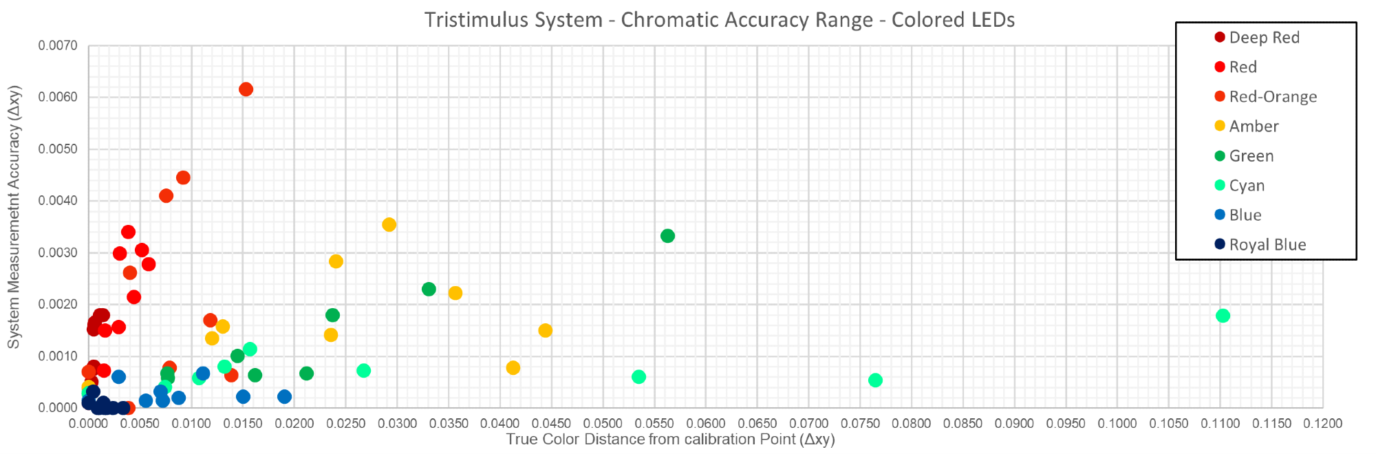
Figure 7. Tristimulus system (ProMetric I29 Imaging Colorimeter) accuracy range for color variation across colored LED test sources. Image Credit: Radiant Vision Systems
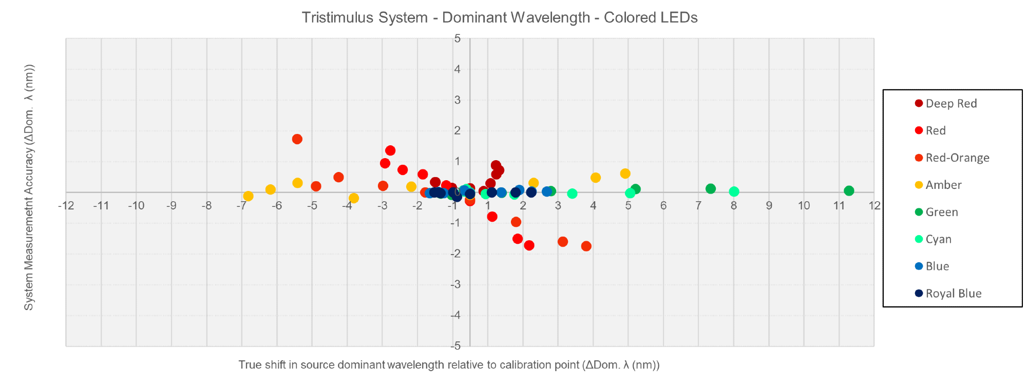
Figure 8. Plot showing true LED source variation at each current level (as measured by the reference spectroradiometer) based on ± nm change in dominant wavelength from the calibration point (x-axis). This axis gives the range of variation observed for each LED. The tristimulus system (ProMetric I29) measurement accuracy is shown as a ± nm difference from the reference measurement at each current level for each LED source (y-axis). Image Credit: Radiant Vision Systems
The Importance of Measurement Accuracy: Pixel-Level Resolution
As previously noted, microLED size span ranges less than 100 µm and as small as 3 µm - about 1/10th the width of a human hair.1 The accuracy of the measurements across a small area of an individual microLED relies on imaging resolution and signal processing methods.
To improve yields through display correction, it is crucial to be able to isolate and measure each singular microLED emitter with a high degree of accuracy for correction of luminance or chromaticity values specific to a given microLED.
A high resolution imaging system maximizes the number of photo-sensing elements (sensor pixels) applied across each microLED for precise subpixel measurements and supplies appropriate resolution to make sure all microLEDs in the display can be measured simultaneously to complete correction processes within adequate cycle times.
Beyond the requirements for display uniformity, visual performance standards in the display industry permit no more than ten dead pixels per display, which can manifest at any point in microLED production.
Guaranteeing microLED display quality necessitates accurate measurement at the LED, chip, wafer and panel stage to limit the potentiality of dead pixels and assess uniformity prior to the introduction of defects at any subsequent stage.
LED, Chip and Wafer-Level Measurement: A high resolution, low noise imaging colorimeter with a standard lens or microscope objective can be utilized for the inspection of individual microLEDs, chips and wafers.
A microscope lens enables 5X or 10X zoom (5 to 10 times the standard resolution of the imaging system across the area of the LED or component), allowing for precise measurements of each singular emissive element (see Figure 9).
Used with a high resolution imaging system, a microscope lens facilitates the capturing of every display subpixel or LED across multiple image sensor pixels for enhanced measurement precision.
Panel-Level Measurement: Once individual microLED chips are positioned onto a backplane, an imaging colorimeter with standard lens can be utilized to simultaneously measure subpixel luminance and chromaticity values across the whole panel.
The benefit of an imaging colorimeter is its capacity to capture a large area in a single image to rapidly assess uniformity with precision, akin to a user viewing the display.
To ensure suitable uniformity correction, high resolution imaging systems must persistently provide pixel- and subpixel-level measurement accuracy, even if there is an increase in the number of pixels per display panel. Higher-resolution displays place a greater demand on even the highest-resolution imaging systems.
Taking advantage of the efficiency of single-image display measurement limits the number of image sensor pixels that can be applied to measure each display pixel, which may impede the accuracy of pixel- and subpixel-level measurement data if there is a failure to apply advanced imaging and signal processing methods.
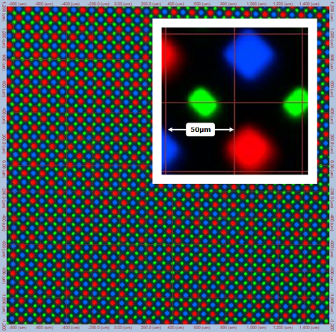
Figure 9. Example of subpixel measurement (main image) taken by a ProMetric I29 Imaging Colorimeter and a Radiant Microscope Lens, magnified to show 50 µm distance at 10X zoom (inset image). Image Credit: Radiant Vision Systems
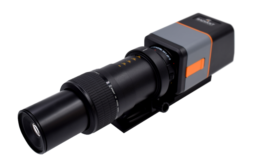
Figure 10. Microscope Lens and ProMetric imaging system from Radiant Vision Systems. Image Credit: Radiant Vision Systems
Methods to Improve Pixel Registration and Measurement
Accurate subpixel-level measurement depends on the capacity of a measurement system to sufficiently isolate each display pixel and accurately evaluate its output value. As detailed above, imaging resolution establishes the number of photo-sensing elements (sensor pixels) at hand to cover each individual display pixel.
The application of more sensor pixels per display pixel expand the granularity of data received by the imaging system for accurate pixel registration and pixel measurement.
As overall resolution increases across the display, there is a reduction in an imaging system’s ability to apply appropriate sensor pixels per display pixel while continuing to record measurements for display pixels on a panel in a single image to ensure efficiency is limited.
Two methods proven to considerably improve an imaging system’s ability to isolate and measure subpixels of progressively high resolution displays for correction have been developed by Radiant Vision Systems: a ‘spaced pixel’ method and a ‘fractional pixel’ method – both are detailed below.
Spaced Pixel Method: The spaced pixel measurement method (US Patent 9135851) enhances the effective resolution of a measurement by only applying the measurement system’s total image sensor resolution across a subset of display pixels at any given time.
The method utilizes a series of dot-matrix test patterns displayed on the screen as part of a measurement sequence. A subset of the display’s pixels is illuminated by each pattern, while the remaining pixels are switched off.
An imaging colorimeter measures the output (chromaticity or luminance) of the ‘on’ pixels for each pattern. A successive test image modifies the matrix to switch off the first set of pixels and switch on the next set of pixels for measurement. This process is duplicated until all pixels in the display have been measured.
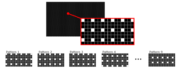
Figure 11. During spaced pixel measurement, a series of dot-matrix patterns illuminates sets of pixels until values have been acquired for all pixels in the display. Image Credit: Radiant Vision Systems
This process enhances the effective resolution of the measurement at each display pixel, establishing the isolation of each pixel’s output and thus the accuracy of measurement calculations across displays of any general resolution.
Images from the spaced pixel measurement method are merged to form a single, synthetic image for analysis, which contrasts values at each of the pixel’s x,y coordinate locations to manage uniformity.
Software calculates the correction coefficient necessary for each display pixel and applies the correction at each pixel’s coordinate location to modify values until display uniformity is achieved.
The spaced pixel method limits the necessity for measurement resolution to enhance measurement accuracy. Yet, due to this method requiring several images, there is also an increase in cycle times.
In contrast, the fractional pixel method (described in the subsequent section) enhances measurement accuracy without increasing cycle times - for instance, only a single measurement image is necessary to assess all pixels across a standard smartphone display.
Thus, the fractional pixel method provides the benefit of shorter cycle times as required, which is the case in numerous production-level test and correction applications.
Fractional Pixel Method: Where imaging sensor resolution per display pixel is restricted, the fractional pixel method (US Patent 10971044) addresses measurement scenarios, allowing measurement systems with standard resolutions to carry on with accurately measuring and correcting today’s high resolution displays, even in a single-image measurement of the complete display.
Firstly, the fractional pixel method maximizes pixel registration. Pixel registration is a technique that dynamically locates and sets a region of interest (ROI) around every pixel in the measurement image. In conventional methods, ROIs are positioned in alignment with the imaging system’s sensor pixel array.
Yet, as there is a continual increase of display resolutions relative to measurement system resolutions, it is increasingly likely that the center of a display pixel will not be aligned with the center of a sensor pixel.
This reduces the ROI’s capacity to suitably cover and isolate each display pixel. Such a misalignment can lead to measurement error. In contrast, using a floating point, the fractional pixel method sets a registration area around each display pixel.
Thus, based on the highest measured luminance across the display pixel, the ROI is aligned to the center of a display pixel.
Secondly, the fractional pixel method maximizes pixel measurement. The fractional pixel method calculates display pixel output values predicated on the fractional area of each sensor pixel contained within the ROI (see Figure 12, right image).
This enhances the accuracy of measured values over conventional ‘whole pixel’ methods that factor values from the whole area of sensor pixels only partially contained within the ROI (see left image, Figure 12).
The fractional pixel method guarantees accuracy of the pixel-level measurements for ultra-high resolution emissive displays surpassing what was previously thought possible using a single-image capture.
Utilizing the fractional pixel method, imaging systems with restricted resolution (relative to display resolution) can effectively measure pixel-level values across a display in a single image, thus improving cycle time without impeding measurement accuracy.
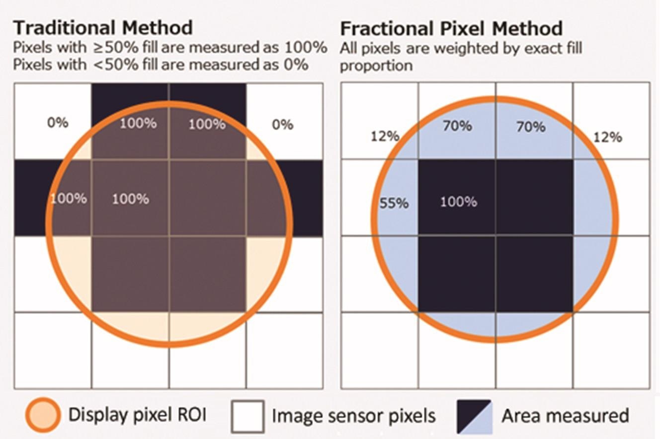
Figure 12. Illustration of a traditional whole pixel measurement method versus the fractional pixel method. In the traditional method (left), display pixels are measured using 100% of the data from sensor pixels whose area is more than 50% inside the ROI and 0% of the data from sensor pixels whose area is less than 50% inside the ROI. Using the fractional pixel method (right), display pixels are measured using a percentage of data based on the percentage of sensor pixel area inside the ROI. Image Credit: Radiant Vision Systems
Measurement Accuracy Study: The Fractional Pixel Method
The fractional pixel method’s accuracy was exhibited in a study published by Pedeville, Rouse and Kreysar (2020).4 Figure 13 plots single-image measurement data from this study, contrasting the pixel-level measurement accuracy of whole pixel measurements, fractional pixel measurements and extremely high resolution reference measurements.
The fractional pixel data closely complies with the reference data, while the whole pixel measurements deviate from the reference data at multiple points.
Figure 14 demonstrates the before-and-after result of an actual measurement and correction (demura) applied by Radiant Vision Systems using a 29MP ProMetric Imaging Photometer; and both spaced and fractional pixel methods for the correction of a microLED microdisplay panel.
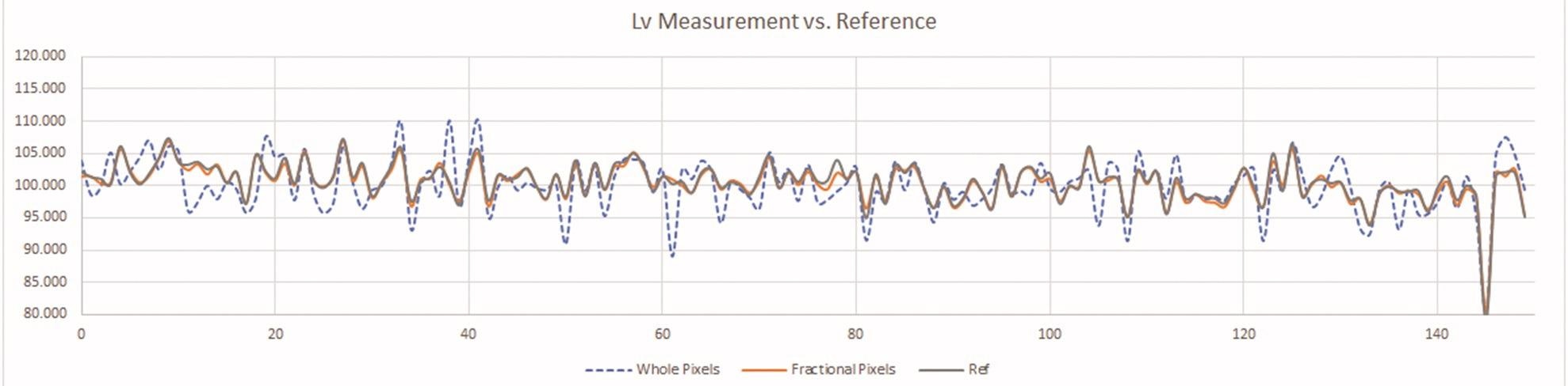
Figure 13. Normalized luminance (Lv) measured by whole and fractional pixel measurement methods (achieving 3.2 x 3.2 sensor pixels per display pixel) and reference luminance (achieving 30 x 30 sensor pixels per display pixel) for the same row of pixels on an emissive display. Image Credit: Radiant Vision Systems
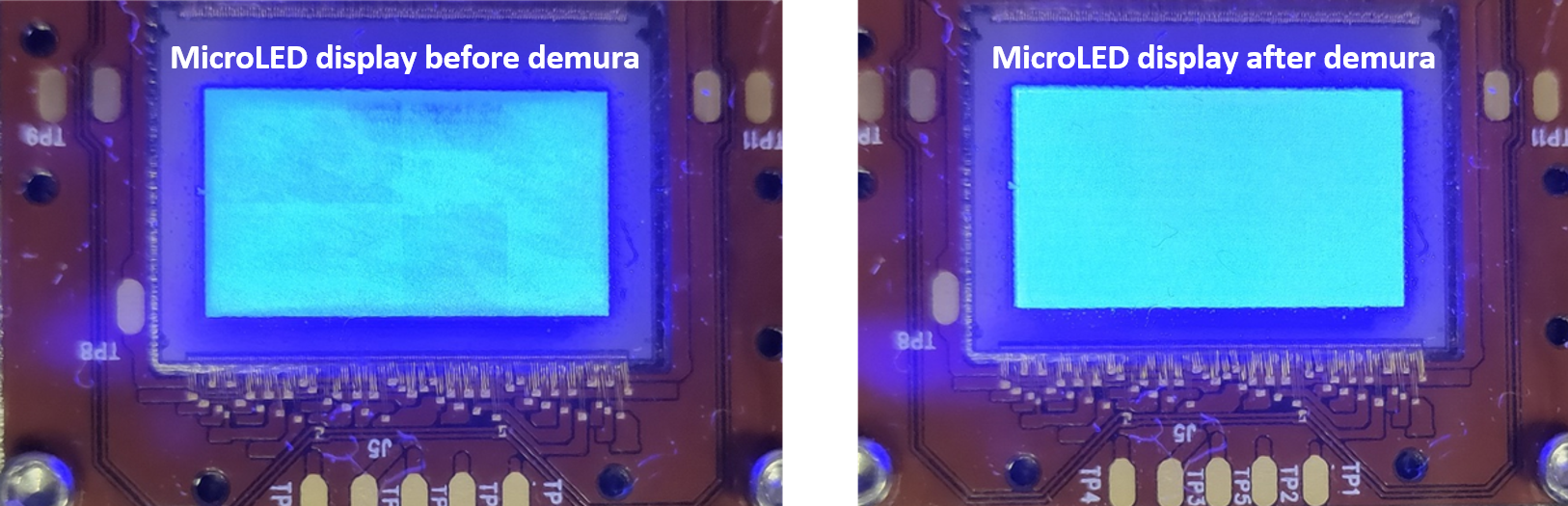
Figure 14. MicroLED microdisplay panel shown before (left) and after (right) demura correction. The panel shown is 0.7” with full HD, 1920 x 1080 and LED size/pitch of 2 µm/8 µm. Measurement and correction were performed using a ProMetric Y29 Imaging Photometer with Microscope Lens and TrueTest™ Software. Image Credit: Radiant Vision Systems
Conclusion
MicroLEDs are rapidly taking their place in the extremely competitive display marketplace. Developers are driven to discovering production solutions that supply high performance and surpass customer expectations while maintaining high yields and cost-efficient production processes.
High resolution tristimulus imaging colorimeter systems offer an effective solution to facilitate quality and efficiency benchmarks for microLED production.
These systems depend on their color filter method, calibrations and subpixel measurement capacities to guarantee accurate data is recorded at the pixel and subpixel level, allowing for correction that safeguards manufacturing resources.
Studies of contemporary display metrology systems and measurement methods show the benefits of high resolution tristimulus imaging systems.
Combined with sophisticated algorithms for calibration, registration and measurement, they solve the challenges faced with microLED display uniformity while supporting the viability of microLED technology for the display device marketplace.
Utilizing imaging colorimeters and novel imaging methods, manufacturers at all stages of microLED manufacture (from LED to wafer to panel) can achieve an appropriate solution for efficient production that facilitates the production of yields with good quality, reduced waste and continual innovation in the development of high performance displays in a range of types, sizes and applications.
References
- Lapedus, M., “MicroLEDs: The Next Revolution in Displays?” Semiconductor Engineering, May 2019. (Retrieved from https://semiengineering.com/microleds-the-next-revolution-in-displays/)
- Carter, E., Schanda, J., Hirschler, R., Jost, S., Luo, M., Melgosa, M., … Wold, J., CIE 015:2018 Colorimetry, 4th Edition, 2018. DOI: 10.25039/tr.015.2018
- Jensen, J., Piehl, A., and Renner, W., “Evaluating tristimulus and Bayer pattern matching system accuracy for color measurement based on CIE color-matching functions,” presented at the 34th annual electronic displays conference (edC), January 2020.
- Pedeville, G., Rouse, J., and Kreysar, D., “Fractional Pixel Method for Improved Pixel-Level Measurement and Correction (Demura) of High Resolution Displays,” Society for Information Display (SID) Display Week 2020 Digest, Book 2, August 2020.

This information has been sourced, reviewed and adapted from materials provided by Konica Minolta Sensing Americas.
For more information on this source, please visit Konica Minolta Sensing Americas.