Mar 16 2020
Silicon photonics is regarded as a vital technology for advanced optical communications at the near-infrared wavelength band of 1.31/1.55 μm.
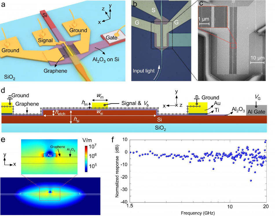 a. Schematic configuration; b. Optical microscope; c. SEM pictures; d. Cross-section of the present silicon-graphene hybrid plasmonic waveguide with the signal electrode at the middle and the ground electrodes at both sides (here the metal-graphene-metal sandwich structure is utilized); e. The electric field component distribution of the quasi-TE0 mode for the optimized silicon-graphene hybrid plasmonic waveguide; f. Measured frequency response of Device B operating at Ë = 2 μm (bias voltage: −0.5 V, gate voltage: 2.9 V). Image Credit: Jingshu Guo, Jiang Li, Chaoyue Liu, Yanlong Yin, Wenhui Wang, Zhenhua Ni, Zhilei Fu, Hui Yu, Yang Xu, Yaocheng Shi, Yungui Ma, Shiming Gao, Liming Tong, and Daoxin Dai.
At present, there is a desire to extend silicon photonics to the wavelength band more than 1.55 μm (for example, 2 μm) for crucial applications in nonlinear photonics, on-chip sensing, and optical communications.
But achieving high-performance silicon-based waveguide photodetectors over 1.55 μm is still difficult, as there exist certain fabrication problems and wavelength-band limitations.
Two-dimensional materials such as graphene offer a potential solution as a substitute due to their potential for wide operation wavelength-bands and the benefit of preventing structure mismatch during design and fabrication.
In a study reported in Light: Science & Applications, researchers from Zhejiang University and Southeast University in China presented and demonstrated high-performance waveguide photodetectors over 1.55 μm, achieved by using a novel silicon-graphene hybrid plasmonic waveguide.
Specifically, an exclusive mode field profile is realized by using an ultra-thin wide silicon ridge core region with a metal cap placed on top. This is performed to improve the light absorption of graphene. Moreover, the fabrication is simple, and the graphene-metal contact resistance is minimized than silicon-graphene hybrid waveguides developed earlier.
For instance, the graphene absorption efficiencies are nearly 54.3% and 68.6% for absorption regions with a length of 20 μm and 50 μm, while performing operations at 1.55 μm and 2 μm, respectively.
The quantified 3 dB-bandwidths for the fabricated photodetectors that work at 2 μm are greater than 20 GHz (restricted by the experimental configuration), and the responsivities are 30–70 mA/W for an input optical power of 0.28 mW under a bias voltage of −0.3 V.
The 3 dB-bandwidth for the photodetectors working at 1.55 μm is greater than 40 GHz (restricted by the experimental configuration), and the quantified responsivity is around 0.4 A/W for an input optical power of 0.16 mW under a bias voltage of −0.3 V.
The mechanisms behind graphene photodetectors have been investigated carefully in this study, and it was observed that the photo-thermoelectric effect is the dominant mechanism for photo-response while working at zero bias voltage.
During the operation of the photodetector at non-zero bias voltages, the dominant mechanism turns out to be the photoconductive or bolometric effect. The detailed analysis enables gaining better insights into the production of photocurrent in the graphene-metal interfaces.
We have proposed and demonstrated high-performance silicon-graphene hybrid plasmonic waveguide photodetectors beyond 1.55 μm. In particular, a novel silicon-graphene hybrid plasmonic waveguide was used by introducing an ultra-thin wide silicon ridge core region with a metal cap atop.
Researchers of the Study, Changchun Institute of Optics, Fine Mechanics and Physics
They added, “The optical modal filed is manipulated in both vertical and horizontal directions. Thus, the light absorption in graphene is enhanced, meanwhile the metal absorption loss is minimized. This greatly helps achieve sufficient light absorption of graphene within a short absorption region.”
The silicon-graphene waveguide photodetectors operating at 2 μm were demonstrated with a 3 dB-bandwidth over 20 GHz. The measured responsivity is 30–70 mA/W at the bias voltage of −0.3 V for input optical power of 0.28 mW. The photodetector at 1.55 μm was also demonstrated with excellent performances. The present work paves the way for achieving high-responsivity and high-speed waveguide photodetectors on silicon for near/mid-infrared wavelength-bands.
Researchers of the Study, Changchun Institute of Optics, Fine Mechanics and Physics
“In future works, more efforts should be given to introduce some special junction structures to minimize the dark current and further extend the operation wavelength-band. Graphene waveguide photodetectors may play an important role in mid-infrared silicon photonics, which will play an important role in time resolved spectroscopy, lab-on-chip sensing, nonlinear photonics, as well as optical communication,” they concluded.
Source: http://english.ciomp.cas.cn/