Jun 7 2022Reviewed by Alex Smith
At Tampere University, a team of photonics researchers has presented a new method to manage a light beam with another beam at ultra-low power via a special plasmonic metasurface in a linear medium. This simple linear switching approach makes nanophotonic devices, like optical computing and communication systems, more energy-efficient as they require low intensity of light.
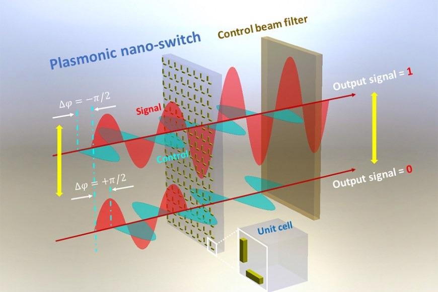
Image Credit: Tampere University
The modulation of signal light by a control light in a way that it has the ON/OFF conversion function is known as all-optical switching. In the presence of a nonlinear medium, a light beam can be modified by another powerful laser beam.
The researchers’ switching approach is based on the quantum optical phenomena known as Enhancement of Index of Refraction (EIR).
Our work is the first experimental demonstration of this effect on the optical system and its utilization for linear all-optical switching.
Humeyra Caglayan, Associate Professor, Photonics, Tampere University
Caglayan added, “The research also enlightens the scientific community to achieve loss-compensated plasmonic devices operating at resonance frequencies through extraordinary enhancement of refractive index without using any gain media or nonlinear processes.”
Optical Switching Enabled with Ultrafast Speed
High-speed switching and low-loss medium to minimize signal degradation during transmission are the foundations for developing integrated photonic technology in which photons are used as information carriers rather than electrons.
All-optical switching should have ultrafast switching time, ultralow threshold control power, ultrahigh switching efficiency, and nanoscale feature size to achieve on-chip ultrafast all-optical switch networks and photonic central processing units.
Switching between signal values of 0 and 1 is fundamental in all digital electronic devices including computers and communication systems. Over the past decades, these electronic elements have gradually become smaller and faster.
Humeyra Caglayan, Associate Professor, Photonics, Tampere University
Caglayan further added, “For example, the ordinary calculations done with our computers on the order of seconds could not be done with old room-sized computers even in several days!”
Switching in traditional electronics is based on managing the flow of electrons on a microsecond (10–6 seconds) or nanosecond (10–9 seconds) time scale by connecting or disconnecting electrical power.
“However, the switching speed can be raised to an ultrafast time scale (femtosecond 10–15 seconds) by replacing the electrons with plasmons. Plasmons are a combination of photons and a collection of electrons on the surface of metals. This enables optical switching with our device with femtosecond (10–15 seconds) speeds”, stated Caglayan.
Our plasmonic nano-switch consists of an L-shaped combination of metallic nanorods. One of the nanorods receives a linearly polarized signal and the other receives another linearly polarized “control” beam perpendicular to the first beam.
Rakesh Dhama, Article First Author and Postdoctoral Research Fellow, Tampere University
Polarization refers to the direction wherein the beam’s electric field oscillates. Depending on the phase difference between the beams, the control beam can suppress or amplify the signal.
The phase difference is the time difference when each beam achieves its greatest intensity. The transfer of some optical energy from the control beam to the signal via a constructive superposition with a properly adjusted phase difference causes signal amplification.
Enhancing the Performance of Plasmonic Devices
The attenuation of the signal is achieved by destructive superposition when the beams have the opposite phase difference. This finding makes nanophotonic devices, including communication systems and optical computing, more sustainable requiring low intensity of light.
By expediting the development and realization of nanoscale plasmonic systems, this simple linear switching approach can replace present ones of optical processing, computing, or communication.
“We expect to see further studies of plasmonic structures utilizing our improved switching method and possibly the use of our method in plasmonic circuits in the future”, noted Caglayan.
She further noted, “Additionally, the L-shaped metasurface could be further studied to reveal ultrahigh-speed switching under the illumination of femtosecond laser pulses and to investigate the nonlinear enhancement and control of plasmonic nanoparticles.”
Managing the nonlinear response of nanostructures gives nanophotonic technologies, such as optical computers and communication systems, considerably more fascinating applications and features.
“This approach has also the potential to enhance the performance of plasmonic devices by creating broadband transparency for a signal beam without any gain medium. It can open up several ways to design smart photonic elements for integrated photonics”, outlined Caglayan.
2020 European Research Council (Starting Grant project aQUARiUM, Academy of Finland Flagship Programme (PREIN), and H2020 Research and Innovation Programme (Marie Skłodowska-Curie MULTIPLY) provided support for the study.
TAU’s Metaplasmonics research group members Rakesh Dhama, Tuomas Pihlava, Dipa Ghindani, and Humeyra Caglayan, as well as guest researcher Ali Panah Pour, conducted the study.
Journal Reference:
Dhama, R., et al. (2022) All-optical switching based on plasmon-induced Enhancement of Index of Refraction. Nature Communications. doi:10.1038/s41467-022-30750-5.
Source: https://www.tuni.fi/en