Researchers from ITMO University, the National University of Colombia, and the University of Siena have developed a two-dimensional structure with unique properties. The discovery will help scientists achieve greater control of electromagnetic surface waves and thus pave the way to compact optical devices for data transfer and processing. The results of the research are published in Physical Review X.
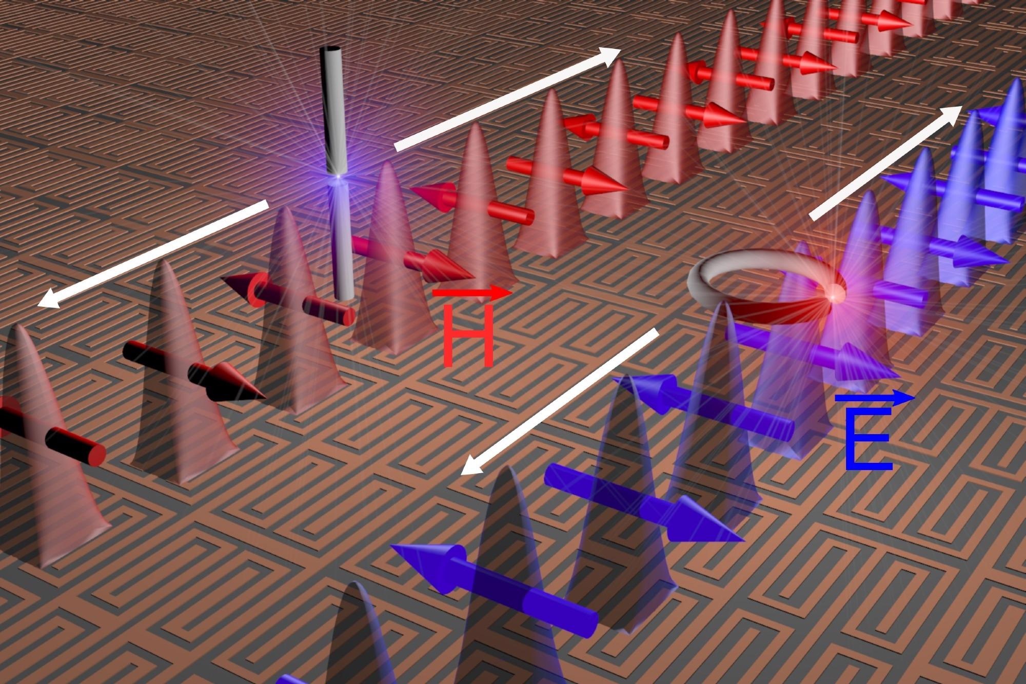
Image Credit: ITMO University
Scholars have studied surface waves for a long time. This phenomenon can be easily observed in real life. One of the vivid examples is circular waves which appear when a stone is thrown into smooth water. From the scientific point of view, surface waves can be potentially used to transmit localized light within a plane and thereby facilitate the development of compact optical and optoelectronic systems for data transmission and processing (antennas, amplifiers, circuits, transmitters, screens, sensors, and even for optical computers). However, researchers encounter several problems when trying to implement this method.
“Surface waves lose nearly all their energy when propagating in various directions at long distances from the source. To that end, scientists found a way to transfer an optical signal from point to point using a canalization effect, which makes waves propagate in a narrow beam along a specific direction. However, scientists find it difficult to change the direction of propagated light in this regime, let alone control the polarization of the waves transmitted in the plane. Light polarization is seen as an optical bit, so its control, basically, allows researchers to “code” information into the light,” explains Oleh Yermakov, a researcher at ITMO’s School of Physics and Engineering.
ITMO scientists managed to solve all these problems using a unique 2D structure. This is a self-complementary metasurface that consists of two mutually inverted components: a dipole antenna and a slit in a metal layer of the same shape.
“Our structure is based on Babinet's principle: its components transform into themselves during inversion, thus revealing rather unique properties. It’s amazing that such a fundamental and long-known optical law helped us develop a fairly simple structure and solve many challenges that scientists have faced for years,” adds Oleh Yermakov.
So far, the developed structure can only be applied at the microwave, terahertz and far-infrared ranges. That is, it can only be reduced by a thousand and not, for example, a million times. Yet the researchers believe that the technology can be implemented in the visible range, too. It can be done with the help of all-dielectric structures. The researchers are currently working towards the development of such structures.
The research was supported by the Russian Science Foundation, the Russian Foundation for Basic Research, and the Foundation for the Advancement of Theoretical Physics and Mathematics “BASIS”.
Source: https://en.itmo.ru/en/