Oct 12 2016
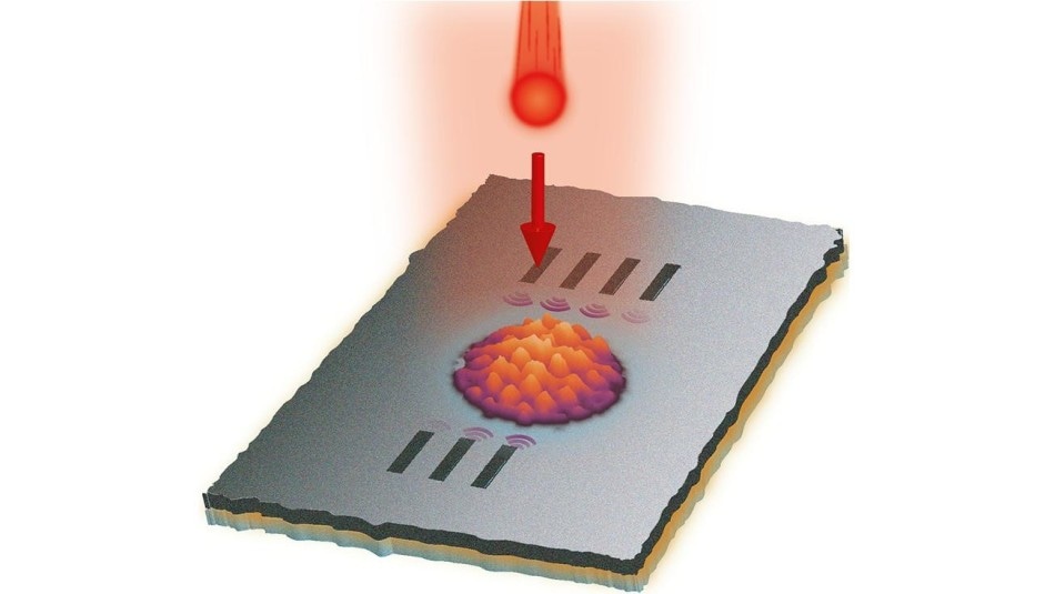 An illustration of the experimental setup © F.Carbone/EPFL
EPFL researchers, who are working to develop potential optical-electronic hybrid computers, have created an ultrafast method that can simultaneously track both light and electrons as they pass through a nanostructured surface.
When both light and electrons come together on a surface, their concentrated motion can move as a wave using the surface geometry. These waves, known as surface plasmons, may be useful in future computing and telecommunications, where data will be transferred across processors by means of light instead of electricity.
These processors, in addition to being more energy efficient, could be reduced to the nanoscale in order to make high-resolution sensors as well as nanosized signal processing systems. However, the processors would be developed from assembling different layers of innovative materials and so far there is no a reliable way to track the guided light when it travels across their interfaces.
Researchers at EPFL have now used a new, ultrafast method to track this process. Their research breakthrough is published in Nature Communications.
Fabrizio Carbone’s lab at EPFL led the research project to develop a small antenna array to allow plasmons to move across an interface. This array is made of a very thin silicon nitride membrane of 50 nm thickness and is covered with a 30 nm thick silver film.
The researchers then “punched” a chain of nano-holes through the surface that may be used as the antennas, the plasmon “hotspots”.
Then, the researchers discharged ultrafast laser pulses (light) on the array in order to light up the antennas. Ultrashort electron pulses were discharged across the multilayer stack with a controlled temporal delay to track the plasmons produced by the antennas during the interaction between the silicon nitride membrane and the silver film.
The researchers used an ultrafast method, named PINEM, to film the transmission of the guided light and interpret its spatial profile across the film. The PINEM method can observe surface plasmons, even when they are attached to a buried interface.
Trying to see plasmons in these interfaces between layers is a bit like trying to film people in a house from the outside. A regular camera won’t show you anything; but if you use microwave or a similar energy-tracking imaging, you can see right through the walls.
Fabrizio Carbone, EPFL
The present research work could lead to designing and managing confined plasmonic fields in complex structures that could be the key for future optical-electronic systems.
This project received support from EPFL’s Interdisciplinary Center for Electron Microscopy, the University of Glasgow, Boston University, the Institució Catalana de Recerca i Estudis Avancats, the Barcelona Institute of Science and Technology, and Trinity College (US). It was funded by the Swiss National Science Foundation (NCCR-MUST), the European Research Council (ERC), Trinity College, MINECO (Spain) and the Connecticut Space Grant Consortium.