May 2 2013
MOSIS, a provider of low-cost prototyping and small volume production services for custom ICs, teams up with ePIXfab, the European Silicon Photonics support center providing low-cost prototyping services for photonic ICs.
The partnership gives MOSIS' customers access to imec’s state-of-the-art fully integrated silicon photonics processes and Tyndall’s advanced silicon photonics packaging technology.
Imec’s silicon photonics platform enables cost-effective R&D of silicon photonic ICs for high-performance optical transceivers (25Gb/s and beyond) for telecom, datacom, and optical sensing for life science applications. The offered integrated components include low-loss waveguides, efficient grating couplers, high-speed silicon electro-optic modulators and high-speed germanium waveguide photo-detectors.
A comprehensive design kit to access imec technologies will be provided. Moreover, the Tyndall National Institute, being a partner of ePIXfab, offers the ability to provide packaged silicon photonics devices. This includes the design and fabrication of custom photonic packages, fiber coupling (single and arrays) and electrical interconnects. Designs rules to support these packaging capabilities will also be provided “Imec’s Silicon Photonics platform provides robust performance, and solutions to integrated photonics products.
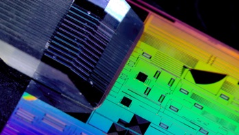 Packaged passive silicon photonics chip. Imec, silicon photonic chip; Tyndall, fiber array packaging.
Companies can benefit from imec silicon photonics capability through established standard cells, or explore the functionality of their own designs in MultiProject Wafer runs,” stated Philippe Absil, program director at imec. “With this collaboration MOSIS will offer its first access to a mature Silicon Photonics infrastructure, with the option for follow on production” added Wes Hansford, MOSIS Director.
The first ePIXfab-Europractice run for passive silicon photonics ICs is open for registration from June 2013 with design deadline September 9th 2013. MOSIS' customers can register for this run and obtain the design kit via MOSIS in June 2013.
Imec’s Si Photonics 200mm wafer platform offers extensive design flexibility and includes:
- Tight within-wafer silicon thickness variation 3sigma < 2.5nm
- 3-level patterning of 220nm top Si layer (193nm optical lithography)
- poly-Si overlay and patterning (193nm optical lithography)
- 3-level n-type implants and 3-level p-type implants in Si
- Ge epitaxial growth on Si and p-type and n-type implants in Ge
- Local NiSi contacts, Tungsten vias and Cu metal interconnects
- Al bond pads
- Validated cell library with fiber couplers, polarization rotators, highly efficient carrier depletion modulators and ultra-compact Ge waveguide photo-detectors with low dark current.
- Design kit support for IPKISS framework, PhoeniX Software and Mentor Graphics software
- Tyndall’s Si Photonics Packaging Technology enables
- Passive device packaging , single and mult-fiber arrays to grating couplers
- Active device packaging, modulators and detectors with electrical ports and fiber arrays
- Custom packaging requirements (mechanical, thermal stability etc.)
About MOSIS
MOSIS is a low-cost prototyping and small-volume production service for VLSI circuit development. Since 1981, MOSIS has fabricated more than 50,000 circuit designs for commercial firms, government agencies, and research and educational institutions around the world. For more information about MOSIS visit the website: http://mosis.com/
About IMEC
Imec performs world-leading research in nanoelectronics. Imec leverages its scientific knowledge with the innovative power of its global partnerships in ICT, healthcare and energy. Imec delivers industry-relevant technology solutions. In a unique high-tech environment, its international top talent is committed to providing the building blocks for a better life in a sustainable society. Imec is headquartered in Leuven, Belgium, and has offices in Belgium, the Netherlands, Taiwan, US, China, India and Japan. Its staff of close to 2,000 people includes more than 600 industrial residents and guest researchers. In 2011, imec's revenue (P&L) was about 300 million euro. Further information on imec can be found at www.imec.be.
Imec is a registered trademark for the activities of IMEC International (a legal entity set up under Belgian law as a "stichting van openbaar nut”), imec Belgium (IMEC vzw supported by the Flemish Government), imec the Netherlands (Stichting IMEC Nederland, part of Holst Centre which is supported by the Dutch Government), imec Taiwan (IMEC Taiwan Co.) and imec China (IMEC Microelectronics (Shangai) Co. Ltd.) and imec India (Imec India Private Limited).
About Tyndall National Institute
The Tyndall National Institute is Ireland’s largest research institute and performs research in the fields of photonics, nanotechnology and microsystems. In photonics, the institute has expertise developing advanced packaging solutions for both InP and Silicon photonic technologies and has a state-of-the-art photonic packaging laboratory.
Tyndall’s photonic packaging capabilities extend from design, including optical, electrical, mechanical and thermal design, through to packaging of prototype and low volumes and reliability testing. Users of Tyndall’s advanced packaging capabilities can avail of standard and custom photonic packaging solutions to meet their particular requirements.
About ePIXfab-Europractice
ePIXfab is the European Silicon Photonics Platform co-funded by the EU. ePIXfab is a consortium of partners coordinated by the Photonics Research Group, Ghent University and imec partnership. Other members of the consortium are CEA-LETI (France), IHP (Germany) TNO (Netherlands), Tyndall (Ireland) , VTT (Finland) and CMC Microsystems (Canada); providing together diverse expertise from design to packaging thus supporting the emergence of a fabless ecosystem in Silicon Photonics.
Mature ePIXfab technologies are accessible through Europractice-IC service. For more information about ePIXfab visit: http://epixfab.eu/. For more information about Europractice visit: http://www.europractice-ic.com/index.php.