Transmission electron microscopy (TEM) – a bespoke tool for materials scientists for decades– is used in almost every technological field of endeavor. There are TEM applications across industry, forensics, and advanced research.
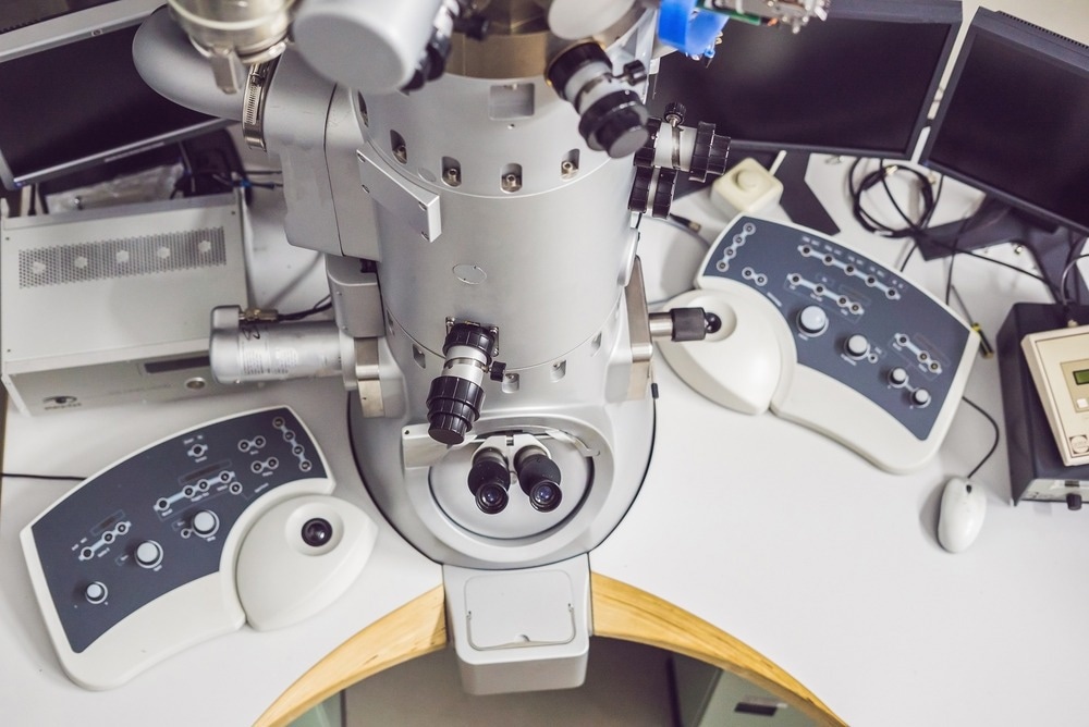
Image Credit: Elizaveta Galitckaia/Shutterstock.com
TEM is the primary high spatial resolution microscopy technique favored by scientists in industry and academia alike. It is used to study quantum dots, cellular 3D tomographic images, and holography. TEM devices made possible our current understanding of photonics, nanotechnology, and biophysics.
What is Transmission Electron Microscopy (TEM)?
Transmission electron microscopy (TEM) uses a beam of electrons to “illuminate” specimens, rather than photons used in traditional optical microscopy. Electrons have a much shorter wavelength than light, enabling TEM devices to magnify images to much higher resolutions.
In TEM, electrons are passed through an ultrathin sample (usually under 100 nm thick) toward a sensor on the other side of the sample. The sensor records electrons that have been scattered through interactions with the sample material, focusing and magnifying this image in an imaging device.
Scattering is caused by the electrostatic potential that emerges from the specimen’s constituent elements and nanostructure.
The basic working principles for TEM are the same as optical microscopy, which focuses on an image through a light-bending lens.
Optical microscopy is limited by the relatively large wavelength of light, whereas electrons’ wavelength is much shorter. This means that TEM is more powerful than optical microscopy can ever be.
TEM devices are used to study nanoscale features of materials, such as their crystal structure, dislocations in the structure, and grain boundaries. In semiconductor material research, for example, TEM is used to study layer growth, composition, and defects.
What is Transmission Electron Microscopy Used For?
Transmission electron microscopy applications are extensive, with the technology finding uses across the sciences and in the industry.
TEM devices deliver information on samples’ topography, morphology, atomic composition, and crystal structures. This information enables researchers to study materials at the level of molecules, analyzing nanoscale structures in the materials.
Physical, chemical, and biological scientists all employ TEM regularly to study the world in its smallest scales. TEM devices are applied in cancer research, virology, and materials science, nanotechnology and semiconductor research, environmental sciences, and even paleontology and palynology.
TEM applications in industry
TEM finds applications in product development and the manufacturing processes of advanced manufacturing sectors such as semiconductors and nanotechnology.
In the electronics industry, TEM devices are used for high-resolution imaging that supports semiconductor development.
TEM can provide a wealth of information about novel semiconductor materials being developed and quality control applications where TEM devices are used to find semiconductor defects and predict their functional ability.
In electronics manufacturing, TEMs may be used to oversee the production of computer processing chips.
Industrial failure analysis, such as forensic science, was revolutionized by introducing TEM and other forms of electron microscopy.
The ability to closely study materials and components, finding smaller than-hairline cracks and defects in materials to better understand reasons for product failure, has enabled much more accurate evaluations of industrial failures.
TEM applications in forensic science
Forensic science is another rich application area for TEM. In forensics, close materials analysis can provide evidence for law enforcement and justice processes.
For example, TEM can be used to analyze gunshot residue, blood found in clothing fibers or items left at crime scenes, and other biological substances that could be used to find DNA and pinpoint the identity of people at the scene.
TEM applications in scientific research
TEM still has a significant role to play in scientific research.
In life sciences, for example, TEM devices are used to study the nature and mechanisms of diseases to provide a better understanding of how to combat them. The entire field of nanotechnology is made possible by TEM’s ultra-high-resolution imagery.
Advantages and Disadvantages of TEM
TEM has numerous advantages that make these applications possible. It offers the strongest magnification over any other magnifying technology. Because of this, TEM devices can give insight into materials’ elements and compound structures.
The images from TEM surveys are of high quality and contain large amounts of detail. This detail includes information about materials’ nanosurface features, shape, size, and molecular structure.
However, there are some disadvantages to the technology, and TEM is not the most suitable microscopy technique for every application.
TEM devices are large, unwieldy, and very expensive. Installing them usually requires bespoke groundworks and often climate-controlled environments so that the device will work properly.
Sample preparation is relatively laborious, requiring scientists to obtain ultra-thin samples of target materials. Sample preparation can also lead to artifacts appearing in the sample, leading to erroneous survey results.
However, if these disadvantages can be overcome, TEM devices will yield the most high-resolution images possible with any current microscopy technology.
References and Further Reading
Montgomery, E., et al. (2021) Ultrafast Transmission Electron Microscopy: Techniques and Applications. [Online] Cambridge University Press. Available at: https://www.cambridge.org/core/journals/microscopy-today/article/ultrafast-transmission-electron-microscopy-techniques-and-applications/FABAA6419FFDE4DC4A670A9EF8DBC4B5 (Accessed on 20 October 2022).
Smith, Y. (2019) Applications of Electron Microscopy. [Online] News Medical. Available at: https://www.news-medical.net/life-sciences/Applications-of-Electron-Microscopy.aspx (Accessed on 20 October 2022).
Transmission Electron Microscope. [Online] Microscope Master. Available at: https://www.microscopemaster.com/transmission-electron-microscope.html (Accessed on 20 October 2022).
Transmission Electron Microscopy (TEM). [Online] University of Warwick. Available at: https://warwick.ac.uk/fac/sci/physics/current/postgraduate/regs/mpagswarwick/ex5/techniques/structural/tem/ (Accessed on 20 October 2022).
Disclaimer: The views expressed here are those of the author expressed in their private capacity and do not necessarily represent the views of AZoM.com Limited T/A AZoNetwork the owner and operator of this website. This disclaimer forms part of the Terms and conditions of use of this website.