Infrared (IR) optical detecting devices such as photodetectors, solar cells, cameras, and microbolometers are shrinking in size, with a tiny effective active area in the micrometer or nanometer range. This article looks at the article titled 'Nano-plasmonic Bundt Optenna for broadband polarization-insensitive and enhanced infrared detection' published in Scientific Reports.

Image Credit: only_kim/Shutterstock.com
Ultrafast optical response, efficient generation/collection of photo-carriers, effective cooling, low operating temperature, small pixel-size for high spatial resolution imaging, and the probability of ultra-dense integration with other devices are all advantages of such a compact size. However, this comes at the cost of the device’s lower aperture area, which results in poor infrared energy collection.
As a result, infrared plasmonic optical antennas come into play because of their capacity to efficiently capture optical energy from a vast free-space area and concentrate it into a compact device.
The optical antenna form should also be constructed to capture optical energy from a big aperture free-space area and confine it down to a sub-wavelength nano-scale area. To achieve an optical-impedance connection between the free-space and detecting device, proper design of the optical antenna shape is required.
Naturally, infrared radiation generates surface plasmon polaritons (SPP) traveling waves on optical antenna, hence a small antenna size is preferable to reduce SPP ohmic power losses on metal surfaces. Furthermore, having a broad bandwidth antenna allows users to take as much energy as possible within a single wavelength range.
Results and Discussion
For the first time in this work, a revolutionary optical-antenna (Optenna) is designed and quantitatively demonstrated. It is in the shape of a Bundt baking-pan.
Figure 1 depicts the schematic diagrams of an infrared detection device with a Bundt optenna on top of a semiconductor thin-film detection layer and a thick bulk substrate that has been widely proposed. As shown in Figure 1a, the optenna is made up of symmetric 2D periodic array of gold Bundt unit-cells.
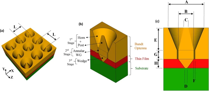
Figure 1. The schematic of the proposed infrared detection device with Bundt optenna. (a) A perspective view of 2D periodic Bundt array, (b) A vertical cross-section of unit-cell indicating different stages and the underneath semiconductor layers, (c) A vertical cross-section of unit-cell indicating different dimensions. Image Credit: Awad, 2019
Over the NIR, SWIR, and MWIR wavelength bands, the Bundt optenna array was evaluated. The Bundt stages’ size has been numerically tuned for the best optical-impedance matching throughout the majority of wavelengths in each band. These designs are shown in Table 1 along with their matching measurements.
Table 1. The four designs of Bundt optenna that can cover the three IR-bands. Source: Awad, 2019
| IR-band |
Band range (µm) |
Design |
A |
B |
C |
D |
E |
G |
L |
| NIR |
0.74–1 |
1 |
0.6 |
0.32 |
0.05 |
0.125 |
1 |
0.5 |
0.625 |
| SWIR |
1–2 |
2 |
1.4 |
0.7 |
0.05 |
0.25 |
2 |
1 |
1.425 |
| 2–3 |
3 |
2 |
1 |
0.1 |
0.35 |
3 |
0.5 |
2.025 |
| MWIR |
3–5 |
4 |
3.2 |
1.6 |
0.2 |
0.55 |
5 |
1 |
3.25 |
When incident infrared light radiation radiates along the negative y-direction, the normalized magnitudes of the electric (magnetic) field of one unit-cell are shown in Figure 2.
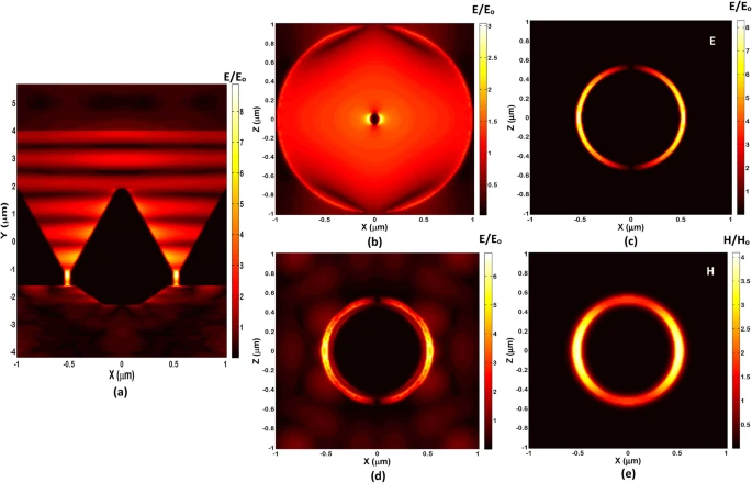
Figure 2. The 3D-FDTD simulations normalized fields within a unit-cell of infrared detection device at a wavelength of 2.3 µm, and TM incident polarization. The normalized electric-field magnitude (E/Eo): (a) A vertical cross-section in a unit-cell, (b) A horizontal cross-section at the input of concentric horn, (c) A horizontal cross-section at the input of annular waveguide, (d) A horizontal cross-section just outside the annular WG (i.e. at entrance of the thin-film layer. The normalized magnetic-field magnitude (H/Ho): (e) A horizontal cross-section at the input of annular waveguide. Image Credit: Awad, 2019
The coupling ratio (CR) of TM-polarized radiation into each Bundt optenna stage is plotted against the appropriate wavelength range in Figure 3.
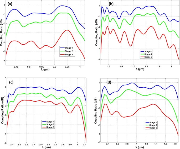
Figure 3. The coupling ratio estimated in decibels of TM-polarized infrared radiation to successive stages of Bundt optenna: (a) Design “1”, (b) Design “2”, (c) Design “3”, (d) Design “4”. Image Credit: Image Credit: Awad, 2019
Table 2 shows the observed bandwidth, estimated center-wavelength, and predicted optical fractional bandwidth for each Bundt design.
Table 2. The wavelength range, bandwidth (BW), and center-wavelength (λo) of different Bundt designs, measured in micrometer (µm). In addition to the percentages of optical fractional bandwidth (O-FBW). Source: Awad, 2019
| IR-band |
Design |
Wavelength range |
BW |
λo |
O-FBW (%) |
| NIR |
1 |
0.71–1.01 |
0.3 |
0.86 |
34.9 |
| SWIR |
2 |
1.43–2.06 |
0.63 |
1.75 |
36 |
| 3 |
2.03–3.12 |
1.1 |
2.58 |
42.6 |
| MWIR |
4 |
3.25–4.86 |
1.61 |
4.06 |
39.7 |
Figure 4 is equivalent to Figure 3, but it shows the normalized intensity at each level instead of the raw intensity. Unlike Figure 3, despite ohmic power loss, this figure indicates an increase in normalized intensity while traveling from stage “1” to “3”.
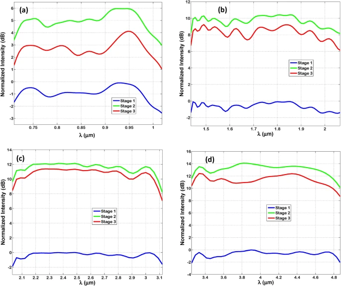
Figure 4. The normalized intensity measured in decibels of TM-polarized infrared radiation at each stage of Bundt optenna: (a) Design “1”, (b) Design “2”, (c) Design “3”, (d) Design “4”. Image Credit: Image Credit: Awad, 2019
In addition to the total power loss, Figure 5 displays the ohmic power losses within every stage of the optenna.
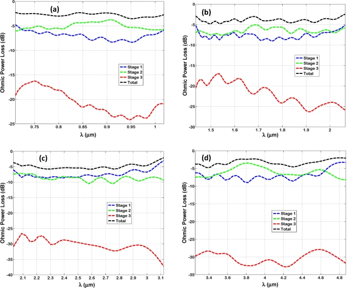
Figure 5. The SPP ohmic power losses measured in decibels of infrared radiation within each stage of Bundt optenna: (a) Design “1”, (b) Design “2”, (c) Design “3”, (d) Design “4”. Image Credit: Awad, 2019
The absorption enhancement factor (EF) within the thin-film layer owing to the Bundt optenna array can be seen in Figure 6. Within the thin-film layer, Figure 7 depicts the estimated photo-generated carrier rate per second.
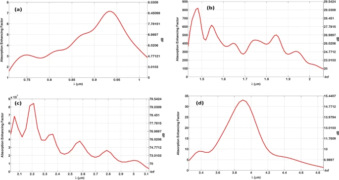
Figure 6. The absorption enhancement factor inside the thin-film layer due to Bundt optenna indicated in linear scale on the left axis, and in decibels on the right axis: (a) Design “1”, (b) Design “2”, (c) Design “3”, (d) Design “4”. Image Credit: Awad, 2019
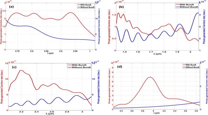
Figure 7. The photo-generated carriers rate (per second) due to optical absorption inside the thin-film layer in case with (red) and without (blue) Bundt optenna: (a) Design “1”, (b) Design “2”, (c) Design “3”, (d) Design “4”. Image Credit: Awad, 2019
Figure 8 illustrates the normalized intensity out of a Bundt optenna as a function of various free-space radiation incidence angles.
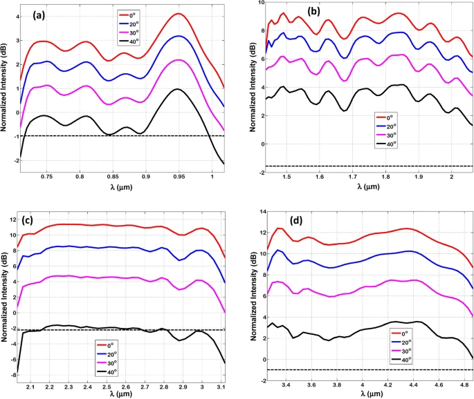
Figure 8. The Normalized intensity out of Bundt optenna as a function of incidence radiation angles: (a) Design “1”, (b) Design “2”, (c) Design “3”, (d) Design “4”. The dashed lines are for the case without Bundt optenna. Image Credit: Awad, 2019
Methodology
The Bundt optenna device simulations were carried out utilizing the Lumerical solutions software program and a three-dimensional finite-difference time-domain approach. A unit-cell including one Bundt optenna, a thin-film absorbing layer, and a substrate is used to imitate the device’s periodic structure, with periodic-Bloch boundary conditions applied to all unit-cell side-walls.
For stabilized simulation, the unit-top cell’s and bottom boundary conditions are set to perfectly matched layers, each with a maximum of 256 layers. During the simulations, some convergent tests were performed to confirm that the numerical errors were acceptable. The coupling ratio’s worst-case inaccuracy was found to be ≅1%, which is considered minimal and acceptable.
Conclusion
The researcher developed a Bundt optical antenna array and numerically demonstrated it for the first time. The Bundt dimensions are optimizable to cover the near, midwave, and shortwave, infrared bands. The Bundt reveals an ultra-broadband optical response harboring high fractional bandwidth of up to 42%. The Bundt optenna is polarization insensitive and has a relatively small size with a reasonable aspect ratio.
It is a better option for various nano-scale infrared detection devices such as photodetectors, solar cells, cameras, and microbolometers, with applications in optical communications, energy harvesting, imaging, sensors, and biomedical technology.
Journal Reference:
Awad, E. (2019) Nano-plasmonic Bundt Optenna for broadband polarization-insensitive and enhanced infrared detection. Scientific Reports, 9, pp. 12197. Available Online: https://www.nature.com/articles/s41598-019-48648-6#citeas.
References and Further Reading
- Schuller, J. A., et al. Plasmonics for extreme light concentration and manipulation. Nature Materials, 9 (3), pp. 193–204. doi.org/10.1038/nmat2630.
- Bharadwaj, P., et al. (2009) Optical Antennas. Advances in Optics and Photonics, 1(3), pp. 438–483.
- Atwater, H A & Polman, A (2010) Plasmonics for improved photovoltaic devices. Nature Materials, 9(2), pp. 205–213. doi.org/10.1038/nmat2629.
- Novotny, L & van Hulst, N (2011) Antennas for light. Nature Photonics, 5 (2), pp. 83–90. doi.org/10.1038/nphoton.2010.237.
- Bonakdar, A & Mohsenim, H (2014) Impact of optical antennas on active optoelectronic devices. Nanoscale, 6 (19), pp. 10961–10974. https://doi.org/10.1039/C4NR02419B.
- Tang, L., et al. Nanometre-scale germanium photodetector enhanced by a near-infrared dipole antenna. Nature Photonics, 2(4), pp. 226–229. doi.org/10.1038/nphoton.2008.30.
- Yang, Y., et al. (2016) Broadband nanophotonic wireless links and networks using on-chip integrated plasmonic antennas. Scientific Reports, 6, p. 19490. doi.org/10.1038/srep19490.
- Andryieuski, A & Malureanu, R (2012) Compact dipole nanoantenna coupler to plasmonic slot waveguide. Optics Letters, 37(6), pp. 1124–1126. doi.org/10.1364/OL.37.001124.
- Thomas, R., et al. (2012) Silicon-based plasmonic coupler. Optics Express, 20(19), 21520–21531. doi.org/10.1364/OE.20.021520.
- Orbons, S. M. et al. (2007) Extraordinary optical transmission with coaxial apertures. Applied Physics Letters, 90(25), p. 251107. doi.org/10.1063/1.2751120.
- Kucherik, A., et al. Nano-Antennas Based on Silicon-Gold Nanostructures. Scientific Reports, 9(1), 338. https://doi.org/10.1038/s41598-018-36851-w.
- Liu, B., et al. (2011) Vertical optical antennas integrated with spiral ring gratings for large local electric field enhancement and directional radiation. Optics Express, 19(11), pp. 10049–10056. doi.org/10.1364/OE.19.010049.
- Caldarola, M., et al. (2015) Non-plasmonic nanoantennas for surface enhanced spectroscopies with ultra-low heat conversion. Nature Communications, 6, p. 7915. doi.org/10.1038/ncomms8915.
- Lin, K. T., et al. (2014) Silicon-based broadband antenna for high responsivity and polarization-insensitive photodetection at telecommunication wavelengths. Nature Communications, p. 3288. doi.org/10.1038/ncomms4288.
- Fang, Z., et al. (2012) Graphene-antenna sandwich photodetector. Nano Letters, 12(7), pp. 3808–3813. doi.org/10.1021/nl301774e.
- Maier, S A (2007) Plasmonics: Fundamentals and Applications. Springer-Verlag, New York, USA.
- de Waele, R., et al. (2009) Plasmon dispersion in coaxial waveguides from single-cavity optical transmission measurements. Nano Letters, 9(8), pp. 2832–2837. https://doi.org/10.1021/nl900597z.
- Polyanskiy, M N (2018) Refractive index database. https://refractiveindex.info.
- Lumerical Solutions, www.lumerical.com.
- Palik, E D (1997) Handbook of Optical Constants of Solids. Academic Press, New York.