Sponsored by PolytecJan 30 2023Reviewed by Maria Osipova
The reliability of a PCB and its respective components, such as an IC (integrated circuit) or a BGA (ball grid array), might differ depending on the design and selection of the semiconductor components that are used. During manufacturing, optimally automated, in-process quality control and validation of the PCB are needed for each kind and series of PCB design.
Furthermore, quality control procedures are utilized at the customer level to identify any “dead on arrival” issues caused, for instance, by breaking on weak points during transit. TopMap optical 3D surface metrology provides areal topography data of PCB, IC, and BGA in a single shot, allowing for quick scanning of full sample surfaces with nanometer resolution.
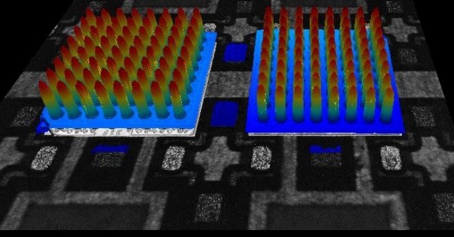
Image Credit: Polytec
Types of Ball Grid Array Packaging
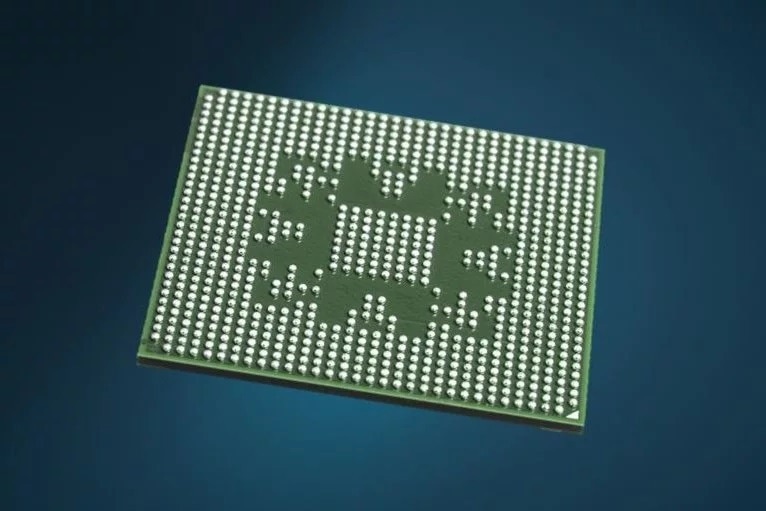
Over the years, there have been several forms of semicon packaging; there were DIPs (dual in-line package), QFP (quad flat package) or QFN (quad flat no leads), and BGA (ball grid arrays) - one of the most common packaging approaches, resulting in an ever-increasing pin count. BGA is prevalent in consumer electronics such as tablets, smartphones, motherboards, and digital cameras.
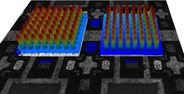
When compared to DIPs and QFPs, BGAs have more I/O connections and shorter connectors, resulting in better performance and speed. The most commonly used bump materials are SnAgCu, SnPb, SnIn, and SnBi, with bump sizes ranging from 90 to 400 µm and the distance between bumps ranging from 0.1 to 2 mm.
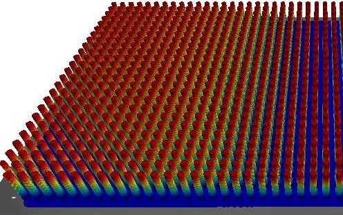
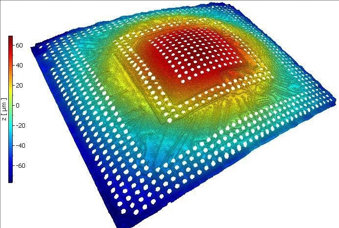
3D profile of a ball grid array pitch measured with optical surface metrology. Image Credit: Polytec
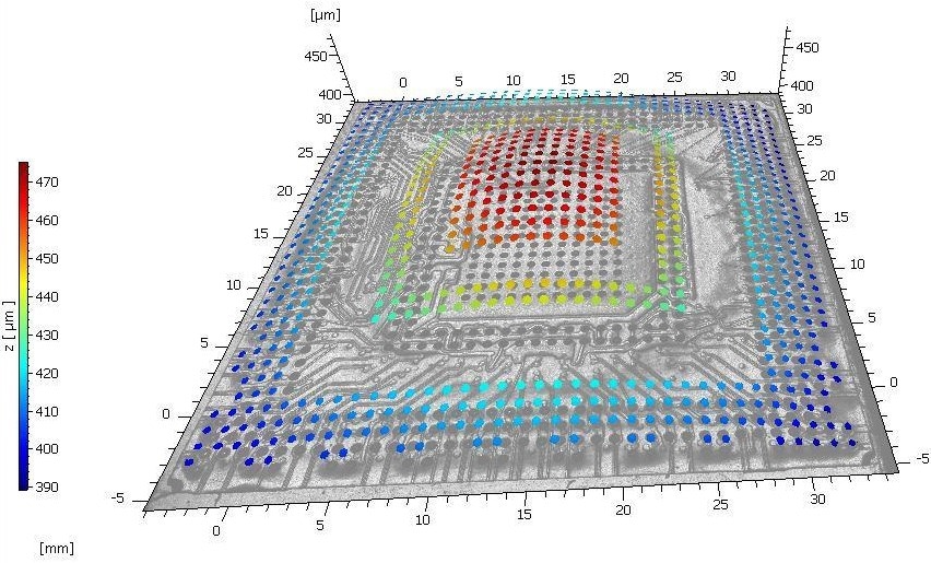
Large field of view measurement and stitching of BGA topography. Image Credit: Polytec
Ball grid array (BGA) bump areal measurement with large field of view. Image Credit: Polytec
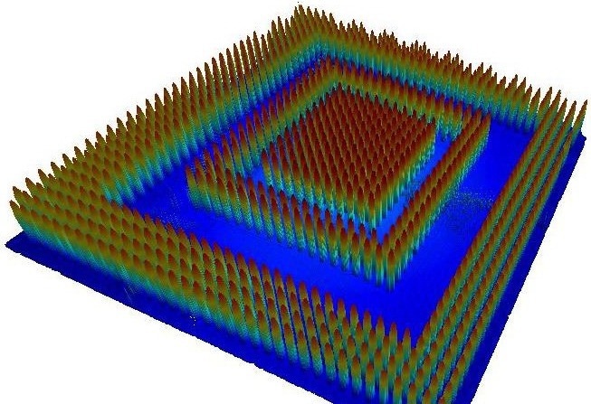
Ball grid array (BGA) bump measurement in 3D. Image Credit: Polytec
Typical Failures and Defects Associated With BGA Manufacturing
In the production of BGAs, for instance, when employing the flip chip approach, which defines the connection by applying pressure and heat to the substrate, common manufacturing faults or defects can occur when the pitch is too high or when the bump is too big or small.
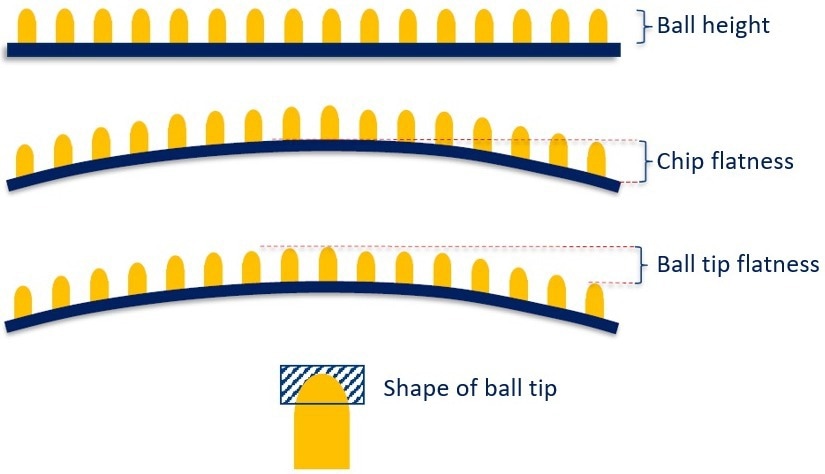
Polytec TopMap surface profilers are appropriate metrology solutions for areal measurement and the examination of coplanarity, ball height/bump height, chip warpage and chip flatness, optical inspection of the complete BGA pitch, BGA ball flatness, or concentrating on the shape of the pure ball tip in an optical and non-contact manner.
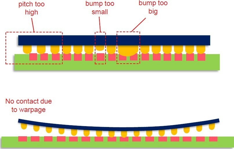
Typical manufacturing problems of BGA and bump height measurement. Image Credit: Polytec
Typical BGA manufacturing issues and optical testing solutions. Image Credit: Polytec
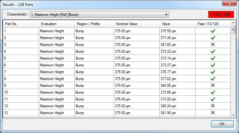
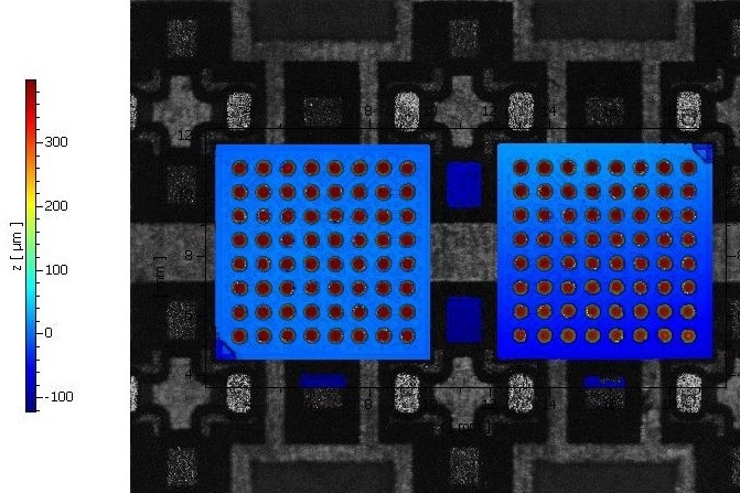
Ball grid array maximum height measurement as pass-fail analysis. Image Credit: Polytec
BGA Warpage and Quality Control
Uncontrolled warpage is another problem associated with the manufacture of BGAs. This phenomenon causes the areal deformation of the entire surface of the PCB or BGA, resulting in disconnected sections and faults on the BGA.
If the warpage is not controlled, even precisely manufactured ball grids will be unable to deliver the functional behavior that is required, resulting in the BGA fitting incorrectly onto the board.
However, optical profilers such as the TopMap white-light interferometers are able to consistently detect warpage in 3D on large areas without contact, meaning that the user can use clear damage identification as useful feedback when it comes to the manufacture of BGAs.
Surface quality control solutions for BGA ball-grid array pins. Image Credit: Polytec
Ball grid array warpage measurement with substracted BGA pins. Image Credit: Polytec
Ball grid array and extracted BGA pin measurement with substracted warpage. Image Credit: Polytec
3D Profiling as Quality Inspection of Ball Grid Arrays
3D optical profilers can be effective quality control devices for areal and non-contact characterization: for testing printed circuit boards (PCBs), detecting solder bumps, assessing the flatness of ball grid arrays, performing pass-fail analyses, and troubleshooting production processes when making PCBs.
Optical profiling can be an essential productive component of the quality control process of electronics and microelectronics, offering useful feedback for the PCB and electronics production processes.
Typically, more complicated and sophisticated PCBs are applied and developed layer by layer, which may require the user to measure the thickness and differentiation between the various layers.
This article outlines some of Polytec’s optical testing solutions that provide a plethora of options for layer thickness measurement as a quality indicator.
Characterization of micro electronics | TopMap - optical 3D surface metrology
Video Credit: Polytec
Further Applications
Die Bonding
Image Credit: Polytec
Flexible Electronics
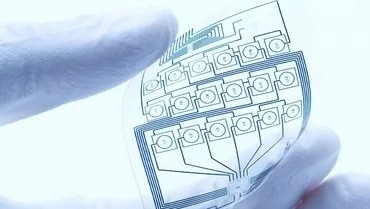
Image Credit: Polytec
High Power Laser Diodes
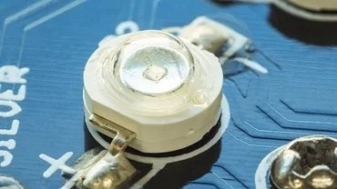
Image Credit: Polytec
Mobile Devices

Image Credit: Polytec
Pass/Fail Analysis
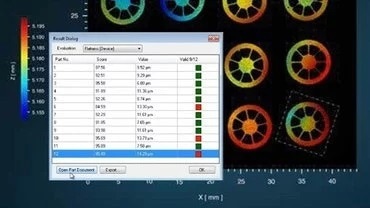
Image Credit: Polytec
Surface Parameters
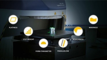
Image Credit: Polytec
This information has been sourced, reviewed and adapted from materials provided by Polytec.
For more information on this source, please visit Polytec.