Jan 13 2016
A unique filtering technology that combines light and sound waves on a single chip is expected to better detect radar and communications frequencies.
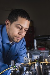 Sandia National Laboratories researcher Charles Reinke studies a tiny phononic/photonic filter nestled among test equipment on a green, stamp-sized substrate toward the picture’s bottom-right. (Photo by Randy Montoya)
“We have developed a powerful signal filtering technology that could revolutionize signal processing systems that rely solely on conventional electronics,” said Patrick Chu, manager of applied photonic microsystems for Sandia National Laboratories.
The radio frequency (RF) filters, which promise both high bandwidth and wide functional flexibility, would form the basis for spectrometers that would let users “see” energies placed in various frequency bands across a wide spectral range.
The novel, very thin filter structures are in the laboratory stage. A system demonstration — complete with lasers, modulators, detectors and battery — should be a bit larger than a computer hard drive, weigh only a few pounds and become available within three to five years.
Photon-to-phonon conversion
The filter uses a relatively new concept called photon/phonon coupling. This technique lets the hybrid device temporarily change RF signals propagating as photons (light) into phonons (sound), enabling efficient analog manipulation of those slower-moving signals.
With this hybrid approach, also known as nano-optomechanical coupling, the researchers were able to combine the high bandwidth offered by light — demonstrated at frequencies up to 20 gigahertz and easily extended to 100 gigahertz — with the linearity and sharp resonances provided by phononic filters. The energy cost of this photon-to-phonon conversion is offset by the high-resolution filter responses that exhibit very little signal distortion over a wide frequency range, says Charles Reinke, who leads the Sandia effort.
Like a tin can telephone
A simple analogy for the photon-phonon information transfer is the tin can telephone: two cans connected by a string that transmits sound between a speaker and listener. The speaker’s cup is like the emitter waveguide; it converts audible sound to vibration in the string. The cup by the ear is the receiver waveguide, which converts the vibration back into sound. The string, representing an engineered material called a phononic crystal, not only carries the message but changes its tone by filtering out high-pitch sounds, a kind of signal processing.
Creating a phononic crystal requires taking a thin film of material, in this case silicon nitride and modifying its mechanical properties by creating patterns on it. The resultant crystal exhibits propagation properties not normally found in nature for mechanical waves like sound, and is dependent on the geometry and pattern of the film.
For the filtering system, two materials are key: silicon nitride to form membranes in which the acoustic signals propagate, and silicon to create waveguides that confine the optical signals. The dual system optimizes the acoustic and optical properties of the device independent of each other.
The photonic-phononic devices also could be incorporated with on-chip photodetectors and other electronics.
A paper published in March 2014 in Nature Communications, “Control of coherent information via on-chip photonic-phononic emitter-receivers,” describes the work, initiated by Sandia’s Laboratory Directed Research and Development office and currently funded for almost $5 million by the Defense Advanced Research Projects Agency (DARPA). Lead researcher Peter Rakich, now a professor at Yale University, began the work at Sandia, and the collaboration continues to evolve with research partners at the University of Texas at Austin and the industrial firm Rockwell Collins. First author Heedeuk Shin, who was a postdoctoral employee at Sandia under Rakich’s mentorship, is a professor at Pohang University of Science and Technology in South Korea.
Sandia National Laboratories is a multi-program laboratory operated by Sandia Corporation, a wholly owned subsidiary of Lockheed Martin Corp., for the U.S. Department of Energy’s National Nuclear Security Administration. With main facilities in Albuquerque, N.M., and Livermore, Calif., Sandia has major R&D responsibilities in national security, energy and environmental technologies and economic competitiveness.
Source: http://www.sandia.gov/