As solar cells have come of age, there has been an increasing demand for photovoltaic modules to become more efficient at solar energy conversion, and cheaper to find their way into households around the globe.
Current high costs of solar energy are directly linked to the relatively low efficiency of modern panels and this, in turn, is influenced by defects within solar cells and panels. Such structural defects may stem from challenges in silicon processing and the quality of crystalline lattices or they may be caused by faulty electrical connections on otherwise functional cells.
To address these issues, an array of photo-emissive diagnostic and quality control tools for solar cell research, based around camera detection systems, has been rapidly developing over the past few years.
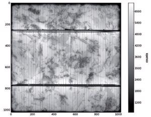
Electroluminescence image of a multicrystalline 12:5 x 12:5 cm2 cell at 20mA/cm2 excitation current density and exposure time of 10s.
Advantages of Electroluminescence Imaging Measurement for PV Quality Inspection
Advantages of electroluminescence imaging measurement for PV Quality Inspection include:
- Analysis and detection of structural defects during production cycle.
- Spatially resolved detection of defects and feedback loops for corrective measures in the production processes.
- High reproducibility of measurement results.
- Speed: fast detection & analysis. <1s.
- Minimizes "down times".
- Fast returns on investment.
- Modular & Flexible: applicable at many stages of production process allowing for flexible reshuffling of resources.
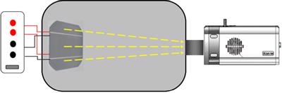
Experimental Set-up
The set-up for PV EL Imaging is simple, consisting of:
- NIR Sensitive Camera with lens
- Darkened enclosure
- Solar Cell / Module
- Power Supply
Detector Requirements
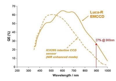
Scientific CCD cameras are very well suited for industrial, inline solar cell quality control processes. CCDs with their two-dimensional array sensors, high Quantum Efficiency (QE), low read noise and down to sub-second frame read out, represent excellent tools for high-throughput testing of individual photovoltaic cells and larger panels.
The sensitivity inherent to CCD-based detection is well placed to harness the phenomenon of induced electroluminescence (EL) from solar cells and modules, utilizing weak emission in the Near Infra-Red (NIR) to detect shunts, crystalline defects and broken finger electrodes during cell manufacturing process.
Electron Multiplying (EM) CCD technology, which combines single photon sensitivity and high QE, offers additional advantages when dealing with low-light EL signals, making it possible to record the faintest of signals. Including CCD / EMCCD technology in solar cell / photovoltaic research can significantly improve the quality of solar panels as well as contribute towards development of cleaner sources of energy.
Andor Product Solutions for Photovoltaic Electroluminescence Imaging
Andor Product Solutions for Photovoltaic Electroluminescence Imaging include:
- Clara Interline CCD
- iKon-M Deep Depletion CCD
- sCMOS Technology

This information has been sourced, reviewed and adapted from materials provided by Andor Technology Ltd.
For more information on this source, please visit Andor Technology Ltd.